DS80C390-QCR Maxim Integrated Products, DS80C390-QCR Datasheet - Page 36
DS80C390-QCR
Manufacturer Part Number
DS80C390-QCR
Description
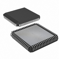
IC MPU CAN DUAL HS 68-PLCC
Manufacturer
Maxim Integrated Products
Series
80Cr
Datasheet
1.DS80C390-FCR.pdf
(53 pages)
Specifications of DS80C390-QCR
Core Processor
8051
Core Size
8-Bit
Speed
40MHz
Connectivity
CAN, EBI/EMI, SIO, UART/USART
Peripherals
Power-Fail Reset, WDT
Number Of I /o
32
Program Memory Type
ROMless
Ram Size
4K x 8
Voltage - Supply (vcc/vdd)
3.85 V ~ 5.5 V
Oscillator Type
External
Operating Temperature
0°C ~ 70°C
Package / Case
68-LCC, 68-PLCC
Processor Series
DS80C390
Core
8051
Data Bus Width
8 bit
Program Memory Size
4 KB
Data Ram Size
4 KB
Interface Type
CAN, IrDA
Maximum Clock Frequency
40 MHz
Number Of Programmable I/os
32
Number Of Timers
3
Operating Supply Voltage
3.85 V to 5.5 V
Maximum Operating Temperature
+ 70 C
Mounting Style
SMD/SMT
3rd Party Development Tools
PK51, CA51, A51, ULINK2
Minimum Operating Temperature
0 C
Lead Free Status / RoHS Status
Contains lead / RoHS non-compliant
Eeprom Size
-
Program Memory Size
-
Data Converters
-
Available stocks
Company
Part Number
Manufacturer
Quantity
Price
Company:

Part Number:
DS80C390-QCR
Manufacturer:
Maxim Integrated
Quantity:
10 000
Company:
Part Number:
DS80C390-QCR+
Manufacturer:
Maxim Integrated Products
Quantity:
135
Company:
Part Number:
DS80C390-QCR+
Manufacturer:
MAXIM
Quantity:
17
Company:
Part Number:
DS80C390-QCR+
Manufacturer:
Maxim Integrated
Quantity:
10 000


Table 8. Program Memory Chip-Enable Boundaries
The DS80C390 incorporates a feature allowing PCE and CE signals to be combined. This is useful when
incorporating modifiable code memory as part of a bootstrap loader or for in-system reprogrammability. Setting the
PDCE3–0 (MCON.3–0) bits causes the corresponding chip-enable signal to function for both MOVC and MOVX
operations. Write access to combined program and data memory blocks is controlled by the WR signal, and read
access is controlled by the PSEN signal. This feature is especially useful if the design achieves in-system
reprogrammability via external flash memory, in which a single device is accessed through both MOVC instructions
(program fetch) and MOVX write operations (updates to code memory). In this case, the internal SRAM is placed in
the program/data configuration and loaded with a small bootstrap loader program stored in the external flash
memory. The device then executes the internal bootstrap loader routine to modify/update the program memory
located in the external flash memory.
STRETCH MEMORY CYCLES
The DS80C390 allows user-application software to select the number of machine cycles it takes to execute a
MOVX instruction, allowing access to both fast and slow off-chip data memory and/or peripherals without glue
logic. High-speed systems often include memory-mapped peripherals such as LCDs or UARTs with slow access
times, so it may not be necessary or desirable to access external devices at full speed. The microprocessor can
perform a MOVX instruction in as little as two machine cycles or as many as twelve machine cycles. Accesses to
internal MOVX SRAM always use two cycles. Note that stretch cycle settings affect external MOVX memory
operations only and that there is no way to slow the accesses to program memory other than to use a slower
crystal (or external clock).
External MOVX timing is governed by the selection of 0 to 7 stretch cycles, controlled by the MD2–MD0 SFR bits in
the clock-control register (CKCON.2–0). A stretch of zero results in a 2-machine cycle MOVX instruction. A stretch
of seven results in a MOVX of 12 machine cycles. Software can dynamically change the stretch value depending
on the particular memory or peripheral being accessed. The default of one stretch cycle allows the use of
commonly available SRAMs without dramatically lengthening the memory access times.
Stretch cycle settings affect external MOVX timing in three gradations. Changing the stretch value from 0 to 1 adds
an additional clock cycle each to the data setup and hold times. When a stretch value of 4 or above is selected, the
interface timing changes dramatically to allow for very slow peripherals. First, the ALE signal is lengthened by 1
machine cycle. This increases the address setup time into the peripheral by this amount. Next, the address is held
on the bus for one additional machine cycle increasing the address hold time by this amount. The WR and RD
signals are then lengthened by a machine cycle. Finally, during a MOVX write the data is held on the bus for one
additional machine cycle, thereby increasing the data hold time by this amount. For every stretch value greater
than 4, the setup and hold times remain constant, and only the width of the read or write signal is increased. These
three gradations are reflected in the AC Electrical Characteristics, where the eight MOVX timing specifications are
represented by only three timing diagrams.
The reset default of one stretch cycle results in a three-cycle MOVX for any external access. Therefore, the default
off-chip RAM access is not at full speed. This is a convenience to existing designs that use slower RAM. When
maximum speed is desired, software should select a stretch value of zero. When using very slow RAM or
peripherals, the application software can select a larger stretch value.
The specific timing of MOVX instructions as a function of stretch settings is provided in the Electrical Specifications
section of this data sheet. As an example,
stretch value.
111(default)
P4CNT.5–3
000
100
101
110
0h–1FFFFh
0h–3FFFFh
0h–7FFFFh
0–FFFFFh
0h–7FFFh
CE0
Table 9
100000h–1FFFFFh
20000h–3FFFFh
40000h–7FFFFh
80000h–FFFFFh
8000h–FFFFh
shows the read and write strobe widths corresponding to each
36 of 53
CE1
200000h–2FFFFFh
100000h–17FFFFh
80000h–BFFFFh
40000h–5FFFFh
10000h–17FFFh
CE2
180000h–1FFFFFh
300000h–3FFFFFh
C0000h–FFFFFh
18000h–1FFFFh
60000h–7FFFFh
CE3
Related parts for DS80C390-QCR
Image
Part Number
Description
Manufacturer
Datasheet
Request
R

Part Number:
Description:
Manufacturer:
Maxim Integrated Products
Datasheet:

Part Number:
Description:
IC MPU CAN DUAL HS 64-LQFP
Manufacturer:
Maxim Integrated Products
Datasheet:
Part Number:
Description:
IC MPU CAN DUAL HS IND 64-LQFP
Manufacturer:
Maxim Integrated Products
Datasheet:

Part Number:
Description:
IC MPU CAN DUAL HS 68-PLCC
Manufacturer:
Maxim Integrated Products
Datasheet:
Part Number:
Description:
IC MPU CAN DUAL HS IND 68-PLCC
Manufacturer:
Maxim Integrated Products
Datasheet:
Part Number:
Description:
IC MPU CAN DUAL HS IND 68-PLCC
Manufacturer:
Maxim Integrated Products
Datasheet:
Part Number:
Description:
IC MPU CAN DUAL HS 64-LQFP
Manufacturer:
Maxim Integrated Products
Datasheet:
Part Number:
Description:
IC MPU CAN DUAL HS IND 64-LQFP
Manufacturer:
Maxim Integrated Products
Datasheet:
Part Number:
Description:
MAX7528KCWPMaxim Integrated Products [CMOS Dual 8-Bit Buffered Multiplying DACs]
Manufacturer:
Maxim Integrated Products
Datasheet:
Part Number:
Description:
Single +5V, fully integrated, 1.25Gbps laser diode driver.
Manufacturer:
Maxim Integrated Products
Datasheet:
Part Number:
Description:
Single +5V, fully integrated, 155Mbps laser diode driver.
Manufacturer:
Maxim Integrated Products
Datasheet:
Part Number:
Description:
VRD11/VRD10, K8 Rev F 2/3/4-Phase PWM Controllers with Integrated Dual MOSFET Drivers
Manufacturer:
Maxim Integrated Products
Datasheet:
Part Number:
Description:
Highly Integrated Level 2 SMBus Battery Chargers
Manufacturer:
Maxim Integrated Products
Datasheet:
Part Number:
Description:
Current Monitor and Accumulator with Integrated Sense Resistor; ; Temperature Range: -40°C to +85°C
Manufacturer:
Maxim Integrated Products
Part Number:
Description:
TSSOP 14/A°/RS-485 Transceivers with Integrated 100O/120O Termination Resis
Manufacturer:
Maxim Integrated Products