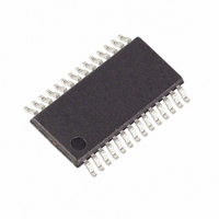
MAXQ3108-FFN+ Maxim Integrated Products, MAXQ3108-FFN+ Datasheet - Page 29

MAXQ3108-FFN+
Manufacturer Part Number
MAXQ3108-FFN+
Description
IC MCU DUAL-CORE 16BIT 28-TSSOP
Manufacturer
Maxim Integrated Products
Series
MAXQ™r
Datasheet
1.MAXQ3108-FFN.pdf
(64 pages)
Specifications of MAXQ3108-FFN+
Core Processor
RISC
Core Size
16-Bit
Speed
10MHz
Connectivity
I²C, SPI, UART/USART
Peripherals
POR, PWM, WDT
Number Of I /o
21
Program Memory Size
64KB (32K x 16)
Program Memory Type
FLASH
Ram Size
11K x 8
Voltage - Supply (vcc/vdd)
1.8 V ~ 3.6 V
Oscillator Type
External
Operating Temperature
-40°C ~ 85°C
Package / Case
28-TSSOP
Processor Series
MAXQ
Core
RISC
Data Bus Width
16 bit
Data Ram Size
2 KB
Interface Type
I2C, JTAG, SPI
Maximum Clock Frequency
10 MHz
Number Of Programmable I/os
22
Number Of Timers
2
Operating Supply Voltage
3.6 V
Maximum Operating Temperature
+ 85 C
Mounting Style
SMD/SMT
Minimum Operating Temperature
- 40 C
Lead Free Status / RoHS Status
Lead free / RoHS Compliant
Eeprom Size
-
Data Converters
-
Lead Free Status / Rohs Status
Lead free / RoHS Compliant
RCNT.6: ALDF
RCNT.7: ALSF
RCNT.8: SQE
RCNT.9: FT
RCNT.[11:10]: 32KMD[1:0]
RCNT.12: 32KBYP
RCNT.13: 32KRDY
RCNT.14: X32D
RCNT.15: WE
______________________________________________________________________________________
Low-Power, Dual-Core Microcontroller
Alarm Time-of-Day Flag. This bit is set when the contents of RTSH and RTSL counter registers
match the 20-bit value in the RASH and RASL alarm registers. Setting the ALDF causes an interrupt
request to the CPU if the ADE is set and interrupt is allowed at the system level. This flag must be
cleared by software once set. This alarm is qualified as a wake up to the stop and the switchback
function if its interrupt has not been masked.
Alarm Subsecond Flag. This bit is set when the subsecond timer has been reloaded by the RSSA
register. Setting the ALSF causes an interrupt request to the CPU if the ASE is set and the interrupt is
allowed at the system level. This flag must be cleared by software once set. This alarm is qualified
as a wake up to the stop and the switchback function if its interrupt have not been masked.
RTC Square-Wave Output Enable. Setting this bit to a logic 1 enables either the 1Hz tap or the
512Hz tap of the RTC to the SQW pin. When cleared to 0, the SQW pin is not driven by the RTC.
Because the P1.3 pin has two possible special function outputs, the SQW special function takes
priority over the JTAG TDO special function output if both are enabled.
RTC Frequency Test. This register bit selects the frequency output that is possible on the SQW pin
if the square-wave output is enabled. Setting FT = 1 selects the 512Hz output (when SQE = 1) while
FT = 0 selects the 1Hz output (when SQE = 1). This bit has no function if the square-wave output is
disabled.
32K Oscillator Mode Bits [1:0]. These two bits determine the 32K oscillator operation modes as
shown in the below table. Changing the value of these bits when the 32K input is enabled (X32D =
0) resets the 32KRDY bit to 0 if the new setting requires the oscillator circuitry to warm up.
32K Bypass Enable. Setting this bit to 1 disables the internal oscillator circuitry connected
between the internal CX1 and CX2 pins. In this configuration, any peripheral that is using the 32K
input can be driven externally by a clock signal provided on the CX1 pin. Clearing this bit to 0
enables the internal crystal oscillator circuitry. When the internal oscillator circuitry is enabled,
250ms are required before the crystal oscillator has warmed up. This bit can only be changed
when RTCE = 0. Note that this bit has no effect when X32D is set to 1.
32K Input Ready. This bit is set to 1 by hardware after the 32K oscillator has warmed up and is
ready to source as input to system clock or peripherals. This bit is cleared to 0 when X32D is set
to 1 or when X32D = 0 and 32KMD values have changed to require the 32K circuitry to warm up.
User application should check that the 32K input is ready (32KRDY = 1) before enabling any
peripherals that use the 32K input as time base; otherwise timing accuracy is compromised. This
bit is read-only.
32K External Input Disable. Setting this bit to 1 disables the 32K circuitry. No external 32K clock
source is accepted. Clearing this bit to 0 enables the 32K circuitry. The source of the input is
configured through the 32KBYP bit. This bit can only be changed when RTCE = 0. Note: If X32D = 0
in stop mode, the 32K source is still available in stop mode.
RTC Write Enable. This register bit serves as a protection mechanism against undesirable writes
to the RTCE bit and RTRM register. This bit must be set to a 1 to give write access to the RTRM
register and the RTCE bit; otherwise (when the WE bit = 0) these protected bits are read-only.
Special Function Register Bit Descriptions (continued)
32KMD[1:0]
00
01
10
11
Always operate in noise immune mode.
Always operate in quiet mode.
Operate in noise immune mode normally, switch to quiet mode on stop
mode entry. On stop mode exit, the CPU code execution must wait for 32K
oscillator to transition (warm up) from quiet mode to noise immune mode.
Operate in noise immune mode normally, switch to quiet mode on stop mode
entry. On stop mode exit, the CPU code execution can occur during the 32K
oscillator transition (warm up) from quiet mode to noise immune mode.
32K OSCILLATOR MODE
29


