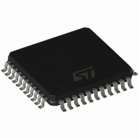
ST72F324J6T6 STMicroelectronics, ST72F324J6T6 Datasheet - Page 150

ST72F324J6T6
Manufacturer Part Number
ST72F324J6T6
Description
IC MCU 8BIT 32K 44-TQFP
Manufacturer
STMicroelectronics
Series
ST7r
Specifications of ST72F324J6T6
Core Processor
ST7
Core Size
8-Bit
Speed
8MHz
Connectivity
SCI, SPI
Peripherals
LVD, POR, PWM, WDT
Number Of I /o
32
Program Memory Size
32KB (32K x 8)
Program Memory Type
FLASH
Ram Size
1K x 8
Voltage - Supply (vcc/vdd)
3.8 V ~ 5.5 V
Data Converters
A/D 12x10b
Oscillator Type
Internal
Operating Temperature
-40°C ~ 85°C
Package / Case
44-TQFP, 44-VQFP
Controller Family/series
ST7
No. Of I/o's
32
Ram Memory Size
1KB
Cpu Speed
8MHz
No. Of Timers
2
Embedded Interface Type
SCI, SPI
No. Of Pwm Channels
1
Rohs Compliant
Yes
Processor Series
ST72F3x
Core
ST7
Data Bus Width
8 bit
Data Ram Size
1024 B
Interface Type
SCI, SPI
Maximum Clock Frequency
8 MHz
Number Of Programmable I/os
32
Number Of Timers
4 bit
Operating Supply Voltage
3.8 V to 5.5 V
Maximum Operating Temperature
+ 85 C
Mounting Style
SMD/SMT
Development Tools By Supplier
ST7F521-IND/USB, ST7232X-EVAL, ST7MDT20-DVP3, ST7MDT20J-EMU3, STX-RLINK
Minimum Operating Temperature
- 40 C
On-chip Adc
10 bit
Cpu Family
ST7
Device Core Size
8b
Frequency (max)
8MHz
Total Internal Ram Size
1KB
# I/os (max)
32
Number Of Timers - General Purpose
2
Operating Supply Voltage (typ)
5V
Operating Supply Voltage (max)
5.5V
Operating Supply Voltage (min)
3.8V
Instruction Set Architecture
CISC
Operating Temp Range
-40C to 85C
Operating Temperature Classification
Industrial
Mounting
Surface Mount
Pin Count
44
Package Type
TQFP
For Use With
497-8222 - UPS (LINE INTERACTIVE - 450W)497-8436 - BOARD EVAL UPS 450W VOUT=220V497-6421 - BOARD EVAL DGTL BATT CHGR DESIGN
Lead Free Status / RoHS Status
Contains lead / RoHS non-compliant
Eeprom Size
-
Lead Free Status / Rohs Status
In Transition
Other names
497-2108
Available stocks
Company
Part Number
Manufacturer
Quantity
Price
Company:
Part Number:
ST72F324J6T6
Manufacturer:
STMicroelectronics
Quantity:
10 000
Part Number:
ST72F324J6T6
Manufacturer:
ST
Quantity:
20 000
Company:
Part Number:
ST72F324J6T6/TR
Manufacturer:
STMicroelectronics
Quantity:
10 000
ST72324Jx ST72324Kx
14 ST72324 DEVICE CONFIGURATION AND ORDERING INFORMATION
14.1 FLASH OPTION BYTES
The option bytes allows the hardware configura-
tion of the microcontroller to be selected. They
have no address in the memory map and can be
accessed only in programming mode (for example
using a standard ST7 programming tool). The de-
fault content of the FLASH is fixed to FFh. To pro-
gram directly the FLASH devices using ICP,
FLASH devices are shipped to customers with the
internal RC clock source.
OPTION BYTE 0
OPT7= WDG HALT Watchdog reset on HALT
This option bit determines if a RESET is generated
when entering HALT mode while the Watchdog is
active.
0: No Reset generation when entering Halt mode
1: Reset generation when entering Halt mode
OPT6= WDG SW Hardware or software watchdog
This option bit selects the watchdog type.
0: Hardware (watchdog always enabled)
1: Software (watchdog to be enabled by software)
OPT5 = Reserved, must be kept at default value.
OPT4:3= VD[1:0] Voltage detection
These option bits enable the voltage detection
block (LVD, and AVD) with a selected threshold for
the LVD and AVD.
150/164
1
Default
7
1
WDG
1
STATIC OPTION BYTE 0
1
1
0
VD
0
0
1
1
1
0
Caution: If the medium or low thresholds are se-
lected, the detection may occur outside the speci-
fied operating voltage range. Below 3.8V, device
operation is not guaranteed. For details on the
AVD and LVD threshold levels refer to
12.4.1 on page 119
OPT2:1 = Reserved, must be kept at default value.
OPT0= FMP_R Flash memory read-out protection
Read-out protection, when selected, provides a
protection against Program Memory content ex-
traction and against write access to Flash memo-
ry.
Erasing the option bytes when the FMP_R option
is selected causes the whole user memory to be
erased first, and the device can be reprogrammed.
Refer to Section 7.3.1 on page 37 and the ST7
Flash Programming Reference Manual for more
details.
0: Read-out protection enabled
1: Read-out protection disabled
Lowest Voltage Threshold (V
Medium Voltage Threshold (V
Highest Voltage Threshold (V
1
7
Selected Low Voltage Detector
1
LVD and AVD Off
STATIC OPTION BYTE 1
OSCTYPE
1
1
0
0
DD
DD
DD
2
1
~3V)
OSCRANGE
~4V)
~3.5V)
1
1
VD1
1
1
0
0
0
1
Section
VD0
0
1
0
1
0
1


