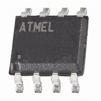
ATTINY13A-SS7 Atmel, ATTINY13A-SS7 Datasheet - Page 54

ATTINY13A-SS7
Manufacturer Part Number
ATTINY13A-SS7
Description
IC MCU AVR 1K FLASH 8SOIC
Manufacturer
Atmel
Series
AVR® ATtinyr
Datasheet
1.ATTINY13A-SSH.pdf
(176 pages)
Specifications of ATTINY13A-SS7
Core Processor
AVR
Core Size
8-Bit
Speed
20MHz
Peripherals
Brown-out Detect/Reset, POR, PWM, WDT
Number Of I /o
6
Program Memory Size
1KB (512 x 16)
Program Memory Type
FLASH
Eeprom Size
64 x 8
Ram Size
64 x 8
Voltage - Supply (vcc/vdd)
1.8 V ~ 5.5 V
Data Converters
A/D 4x10b
Oscillator Type
Internal
Operating Temperature
-40°C ~ 105°C
Package / Case
8-SOIC (3.9mm Width)
Processor Series
ATtiny
Core
AVR
Data Bus Width
8 bit
Data Ram Size
64 B
Interface Type
SPI
Maximum Clock Frequency
20 MHz
Number Of Programmable I/os
6
Number Of Timers
1
Operating Supply Voltage
3.3 V
Maximum Operating Temperature
+ 105 C
Mounting Style
SMD/SMT
Minimum Operating Temperature
- 40 C
Operating Temperature Range
- 40 C to + 105 C
Lead Free Status / RoHS Status
Lead free / RoHS Compliant
Connectivity
-
Lead Free Status / Rohs Status
Details
Available stocks
Company
Part Number
Manufacturer
Quantity
Price
Company:
Part Number:
ATTINY13A-SS7R
Manufacturer:
Atmel
Quantity:
8 052
10.2.6
10.3
54
Alternate Port Functions
ATtiny13A
Unconnected Pins
If a logic high level (“one”) is present on an asynchronous external interrupt pin configured as
“Interrupt on Rising Edge, Falling Edge, or Any Logic Change on Pin” while the external interrupt
is not enabled, the corresponding External Interrupt Flag will be set when resuming from the
above mentioned Sleep mode, as the clamping in these sleep mode produces the requested
logic change.
If some pins are unused, it is recommended to ensure that these pins have a defined level. Even
though most of the digital inputs are disabled in the deep sleep modes as described above, float-
ing inputs should be avoided to reduce current consumption in all other modes where the digital
inputs are enabled (Reset, Active mode and Idle mode).
The simplest method to ensure a defined level of an unused pin, is to enable the internal pull-up.
In this case, the pull-up will be disabled during reset. If low power consumption during reset is
important, it is recommended to use an external pull-up or pull-down. Connecting unused pins
directly to V
accidentally configured as an output.
Most port pins have alternate functions in addition to being general digital I/Os.
shows how port pin control signals from the simplified
by alternate functions.
Figure 10-5. Alternate Port Functions
Note:
WRx, WPx, WDx, RRx, RPx, and RDx are common to all pins within the same port. clk
and PUD are common to all ports. All other signals are unique for each pin.
CC
or GND is not recommended, since this may cause excessive currents if the pin is
PTOExn:
PUOExn:
PUOVxn:
DDOExn:
DDOVxn:
PVOExn:
PVOVxn:
DIEOExn: Pxn DIGITAL INPUT-ENABLE OVERRIDE ENABLE
DIEOVxn: Pxn DIGITAL INPUT-ENABLE OVERRIDE VALUE
SLEEP:
Pxn
Pxn, PORT TOGGLE OVERRIDE ENABLE
Pxn PULL-UP OVERRIDE ENABLE
Pxn PULL-UP OVERRIDE VALUE
Pxn DATA DIRECTION OVERRIDE ENABLE
Pxn DATA DIRECTION OVERRIDE VALUE
Pxn PORT VALUE OVERRIDE ENABLE
Pxn PORT VALUE OVERRIDE VALUE
SLEEP CONTROL
1
0
1
0
1
0
1
0
PUOExn
PUOVxn
DDOExn
DDOVxn
PVOExn
PVOVxn
DIEOExn
DIEOVxn
SLEEP
SYNCHRONIZER
D
L
SET
CLR
Q
Q
PUD:
WDx:
RDx:
RRx:
WRx:
RPx:
WPx:
clk
DIxn:
AIOxn:
D
PINxn
CLR
I/O
Q
Q
:
PORTxn
RESET
Q
Q
CLR
D
RESET
Figure 10-2 on page 50
Q
Q
DDxn
CLR
WRITE DDRx
WRITE PORTx
D
PULLUP DISABLE
READ DDRx
READ PORTx REGISTER
READ PORTx PIN
WRITE PINx
I/O CLOCK
DIGITAL INPUT PIN n ON PORTx
ANALOG INPUT/OUTPUT PIN n ON PORTx
1
0
RRx
clk
PUD
WDx
RDx
DIxn
AIOxn
RPx
I/O
WRx
PTOExn
WPx
can be overridden
8126E–AVR–07/10
Figure 10-5
I/O
, SLEEP,


