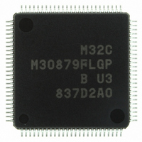
M30879FLGP#U3 Renesas Electronics America, M30879FLGP#U3 Datasheet - Page 597

M30879FLGP#U3
Manufacturer Part Number
M30879FLGP#U3
Description
IC M32C/87 MCU FLASH 100LQFP
Manufacturer
Renesas Electronics America
Series
M16C™ M32C/80r
Specifications of M30879FLGP#U3
Core Size
16/32-Bit
Program Memory Size
1MB (1M x 8)
Core Processor
M32C/80
Speed
32MHz
Connectivity
CAN, EBI/EMI, I²C, IEBus, IrDA, SIO, UART/USART
Peripherals
DMA, POR, PWM, WDT
Number Of I /o
85
Program Memory Type
FLASH
Ram Size
48K x 8
Voltage - Supply (vcc/vdd)
3 V ~ 5.5 V
Data Converters
A/D 26x10b; D/A 2x8b
Oscillator Type
Internal
Operating Temperature
-40°C ~ 85°C
Package / Case
100-LQFP
Controller Family/series
M32C
No. Of I/o's
85
Ram Memory Size
48KB
Cpu Speed
32MHz
No. Of Timers
2
Digital Ic Case Style
LQFP
Embedded Interface Type
CAN, I2C, UART
Rohs Compliant
Yes
Lead Free Status / RoHS Status
Lead free / RoHS Compliant
For Use With
R0K330879S001BE - KIT DEV RSK M32C/87R0K330879S000BE - KIT DEV RSK M32C/87
Eeprom Size
-
Lead Free Status / RoHS Status
Lead free / RoHS Compliant, Lead free / RoHS Compliant
Available stocks
Company
Part Number
Manufacturer
Quantity
Price
Part Number:
M30879FLGP#U3M30879FLGP#U5
Manufacturer:
Renesas Electronics America
Quantity:
10 000
- Current page: 597 of 629
- Download datasheet (16Mb)
M32C/87 Group (M32C/87, M32C/87A, M32C/87B)
REJ09B0180-0151 Rev.1.51 Jul 31, 2008
Page 573 of 587
28.11 Serial Interfaces
28.11.1 Changing UiBRG Register (i = 0 to 6)
28.11.2 Clock Synchronous Mode
28.11.3 UART Mode
28.11.4 Special Mode 1 (I
28.11.2.1 Selecting External Clock
28.11.2.2 Receive Operation
•
•
•
Set the UiBRG register after setting bits CLK1 and CLK0 in the UiC0 register. When bits CLK1 and CLK0 are
changed, set the UiBRG register again.
If an external clock is selected, meet the following conditions while the external clock is held “H” when the
CKPOL bit in the UiC0 register (i = 0 to 6) is set to 0 (transmit data output at the falling edge and receive data
input at the rising edge of the serial clock), or while the external clock is held “L” when the CKPOL bit is set to
1 (transmit data output at the rising edge and receive data input at the falling edge of the serial clock)
Set the UmERE bit in the UmC1 register after setting the UmMR register.
To generate the start condition, stop condition, or restart condition, set the STSPSEL bit in the UmSMR4
register to 0. Then, wait for a half clock cycle of the serial clock or more to change individual condition
generation bit (the STAREQ bit, STPREQ bit, or RSTAREQ bit) from 0 to 1.
(Technical update: TN-16C-130A/EA)
In clock synchronous mode, the serial clock is controlled by the transmit control circuit. Set the UARTi-
associated registers for a transmit operation as well, even if the MCU is used only for receive operation.
Dummy data is output from the TXDi pin while receiving if the TXDi pin is set to output mode.
If data is received continuously, an overrun error occurs when the RI bit in the UiC1 register is 1 (data in the
UiRB register) and the seventh bit of the next data is received in the UARTi receive shift register. And the
OER bit in the UiRB register becomes 1 (overrun error). In this case, a read from the UiRB register returns
undefined values. If an overrun error occurs, the IR bit in the SmRIC register (m = 0 to 4), the U5RR in the
IIO0IR register, or U6RR bit in the IIO9IR register is not changed to 1.
The following two conditions must be satisfied to use continuous receive mode (UiRRM bit is set to 1).
To receive data continuously under the other conditions, set the UiRRM bit to 0 (continuous receive mode
disabled), and write dummy data to the UiTB register every time a receive operation is completed.
The RE bit setting is not required for a transmit-only operation.
•
•
•
(1) The CKDIR bit in the UiMR register is set to 1 (external clock).
(2) The RTS function is not used.
Set the TE bit in the UiC1 register to 1 (transmit operation enabled).
Set the RE bit in the UiC1 register to 1 (receive operation enabled).
The TI bit in the UiC1 register is 0 (data in the UiTB register).
2
C Mode)
28. Usage Notes
Related parts for M30879FLGP#U3
Image
Part Number
Description
Manufacturer
Datasheet
Request
R

Part Number:
Description:
KIT STARTER FOR M16C/29
Manufacturer:
Renesas Electronics America
Datasheet:

Part Number:
Description:
KIT STARTER FOR R8C/2D
Manufacturer:
Renesas Electronics America
Datasheet:

Part Number:
Description:
R0K33062P STARTER KIT
Manufacturer:
Renesas Electronics America
Datasheet:

Part Number:
Description:
KIT STARTER FOR R8C/23 E8A
Manufacturer:
Renesas Electronics America
Datasheet:

Part Number:
Description:
KIT STARTER FOR R8C/25
Manufacturer:
Renesas Electronics America
Datasheet:

Part Number:
Description:
KIT STARTER H8S2456 SHARPE DSPLY
Manufacturer:
Renesas Electronics America
Datasheet:

Part Number:
Description:
KIT STARTER FOR R8C38C
Manufacturer:
Renesas Electronics America
Datasheet:

Part Number:
Description:
KIT STARTER FOR R8C35C
Manufacturer:
Renesas Electronics America
Datasheet:

Part Number:
Description:
KIT STARTER FOR R8CL3AC+LCD APPS
Manufacturer:
Renesas Electronics America
Datasheet:

Part Number:
Description:
KIT STARTER FOR RX610
Manufacturer:
Renesas Electronics America
Datasheet:

Part Number:
Description:
KIT STARTER FOR R32C/118
Manufacturer:
Renesas Electronics America
Datasheet:

Part Number:
Description:
KIT DEV RSK-R8C/26-29
Manufacturer:
Renesas Electronics America
Datasheet:

Part Number:
Description:
KIT STARTER FOR SH7124
Manufacturer:
Renesas Electronics America
Datasheet:

Part Number:
Description:
KIT STARTER FOR H8SX/1622
Manufacturer:
Renesas Electronics America
Datasheet:

Part Number:
Description:
KIT DEV FOR SH7203
Manufacturer:
Renesas Electronics America
Datasheet:


