M30879FLGP#U3 Renesas Electronics America, M30879FLGP#U3 Datasheet - Page 325
M30879FLGP#U3
Manufacturer Part Number
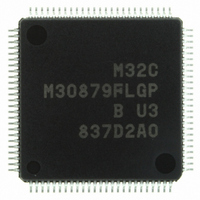
M30879FLGP#U3
Description
IC M32C/87 MCU FLASH 100LQFP
Manufacturer
Renesas Electronics America
Series
M16C™ M32C/80r
Specifications of M30879FLGP#U3
Core Size
16/32-Bit
Program Memory Size
1MB (1M x 8)
Core Processor
M32C/80
Speed
32MHz
Connectivity
CAN, EBI/EMI, I²C, IEBus, IrDA, SIO, UART/USART
Peripherals
DMA, POR, PWM, WDT
Number Of I /o
85
Program Memory Type
FLASH
Ram Size
48K x 8
Voltage - Supply (vcc/vdd)
3 V ~ 5.5 V
Data Converters
A/D 26x10b; D/A 2x8b
Oscillator Type
Internal
Operating Temperature
-40°C ~ 85°C
Package / Case
100-LQFP
Controller Family/series
M32C
No. Of I/o's
85
Ram Memory Size
48KB
Cpu Speed
32MHz
No. Of Timers
2
Digital Ic Case Style
LQFP
Embedded Interface Type
CAN, I2C, UART
Rohs Compliant
Yes
Lead Free Status / RoHS Status
Lead free / RoHS Compliant
For Use With
R0K330879S001BE - KIT DEV RSK M32C/87R0K330879S000BE - KIT DEV RSK M32C/87
Eeprom Size
-
Lead Free Status / RoHS Status
Lead free / RoHS Compliant, Lead free / RoHS Compliant
Available stocks
Company
Part Number
Manufacturer
Quantity
Price

Part Number:
M30879FLGP#U3M30879FLGP#U5
Manufacturer:
Renesas Electronics America
Quantity:
10 000


M32C/87 Group (M32C/87, M32C/87A, M32C/87B)
REJ09B0180-0151 Rev.1.51 Jul 31, 2008
Page 301 of 587
18.1.1
Table 18.4
Function
Analog input pins
Start Condition
Stop condition
Interrupt request generation timing When the A/D conversion is completed
Reading A/D conversion result
In one-shot mode, analog voltage applied to a selected pin is converted to a digital code once. Table 18.4 lists
specifications of one-shot mode.
One-Shot Mode
Item
One-Shot Mode Specifications
Analog voltage applied to a selected pin is converted once
Select one pin from AN_0 to AN_7, AN0_0 to AN0_7, AN2_0 to AN2_7, AN15_0
to AN15_7, ANEX0, or ANEX1
The following register settings determine which pin is used:
• Bits CH2 to CH0 in the AD0CON0 register
• Bits OPA1 and OPA0 in the AD0CON1 register
• Bits APS1 and APS0 in the AD0CON2 register
Software trigger is selected (TRG bit in the AD0CON0 register = 0):
• The ADST bit in the AD0CON0 register is set to 1 (A/D conversion starts)
External trigger, hardware trigger is selected (TRG bit = 1):
• TRG0 bit in the AD0CON2 register = 0
• TRG0 bit = 1
• A/D conversion is completed (the ADST bit becomes 0 when software trigger is
• Set the ADST bit to 0 by a program (A/D conversion stops).
• DMAC operating mode is not used (DUS bit in the AD0CON3 register = 0):
• DMAC operating mode is used (DUS bit = 1):
The falling edge is detected on the ADTRG pin after the ADST bit is set to 1
Timer B2 interrupt request of three-phase motor control timer function (after
the ICTB2 register completes counting) is generated after the ADST bit is set
to 1.
selected).
Read the AD0j register (j = 0 to 7) corresponding to a selected pin by a
program.
A/D conversion result is stored into the AD00 register after A/D conversion is
completed. Then, DMAC transfers the data from the AD00 register to a given
memory space. (Refer to 13. DMAC for DMAC settings)
Specification
18. A/D Converter
Related parts for M30879FLGP#U3
Image
Part Number
Description
Manufacturer
Datasheet
Request
R

Part Number:
Description:
KIT STARTER FOR M16C/29
Manufacturer:
Renesas Electronics America
Datasheet:

Part Number:
Description:
KIT STARTER FOR R8C/2D
Manufacturer:
Renesas Electronics America
Datasheet:

Part Number:
Description:
R0K33062P STARTER KIT
Manufacturer:
Renesas Electronics America
Datasheet:

Part Number:
Description:
KIT STARTER FOR R8C/23 E8A
Manufacturer:
Renesas Electronics America
Datasheet:

Part Number:
Description:
KIT STARTER FOR R8C/25
Manufacturer:
Renesas Electronics America
Datasheet:

Part Number:
Description:
KIT STARTER H8S2456 SHARPE DSPLY
Manufacturer:
Renesas Electronics America
Datasheet:

Part Number:
Description:
KIT STARTER FOR R8C38C
Manufacturer:
Renesas Electronics America
Datasheet:

Part Number:
Description:
KIT STARTER FOR R8C35C
Manufacturer:
Renesas Electronics America
Datasheet:

Part Number:
Description:
KIT STARTER FOR R8CL3AC+LCD APPS
Manufacturer:
Renesas Electronics America
Datasheet:
Part Number:
Description:
KIT STARTER FOR RX610
Manufacturer:
Renesas Electronics America
Datasheet:

Part Number:
Description:
KIT STARTER FOR R32C/118
Manufacturer:
Renesas Electronics America
Datasheet:

Part Number:
Description:
KIT DEV RSK-R8C/26-29
Manufacturer:
Renesas Electronics America
Datasheet:

Part Number:
Description:
KIT STARTER FOR SH7124
Manufacturer:
Renesas Electronics America
Datasheet:

Part Number:
Description:
KIT STARTER FOR H8SX/1622
Manufacturer:
Renesas Electronics America
Datasheet:

Part Number:
Description:
KIT DEV FOR SH7203
Manufacturer:
Renesas Electronics America
Datasheet: