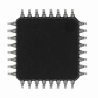
M37544G2AGP#U0 Renesas Electronics America, M37544G2AGP#U0 Datasheet - Page 33

M37544G2AGP#U0
Manufacturer Part Number
M37544G2AGP#U0
Description
IC 740 MCU OTP 8K 32LQFP
Manufacturer
Renesas Electronics America
Series
740/38000r
Specifications of M37544G2AGP#U0
Core Processor
740
Core Size
8-Bit
Speed
8MHz
Connectivity
SIO, UART/USART
Peripherals
WDT
Number Of I /o
25
Program Memory Size
8KB (8K x 8)
Program Memory Type
QzROM
Ram Size
256 x 8
Voltage - Supply (vcc/vdd)
4 V ~ 5.5 V
Data Converters
A/D 6x8b
Oscillator Type
Internal
Operating Temperature
-20°C ~ 85°C
Package / Case
32-LQFP
Lead Free Status / RoHS Status
Lead free / RoHS Compliant
Eeprom Size
-
Available stocks
Company
Part Number
Manufacturer
Quantity
Price
Rev.1.04
REJ03B0012-0104Z
7544 Group
A/D Converter
The functional blocks of the A/D converter are described below.
[A/D conversion register] AD
The A/D conversion register is a read-only register that stores the
result of A/D conversion. Do not read out this register during an A/
D conversion.
[A/D control register] ADCON
The A/D control register controls the A/D converter. Bit 2 to 0 are
analog input pin selection bits. Bit 4 is the AD conversion comple-
tion bit. The value of this bit remains at “0” during A/D conversion,
and changes to “1” at completion of A/D conversion.
A/D conversion is started by setting this bit to “0”.
[Comparison voltage generator]
The comparison voltage generator divides the voltage between
AV
[Channel selector]
The channel selector selects one of ports P2
and inputs the voltage to the comparator.
[Comparator and control circuit]
The comparator and control circuit compares an analog input volt-
age with the comparison voltage and stores its result into the A/D
conversion register. When A/D conversion is completed, the con-
trol circuit sets the AD conversion completion bit and the AD
interrupt request bit to “1”. Because the comparator is constructed
linked to a capacitor, set f(X
version.
Fig. 34 Block diagram of A/D converter
SS
and V
REF
2004.06.08
Data bus
by 256, and outputs the divided voltages.
P2
P2
P2
P2
P2
P2
0
1
2
3
4
5
/AN
/AN
/AN
/AN
/AN
/AN
A/D control register
0
1
2
3
4
5
(Address 0034
IN
page 31 of 66
) to 500 kHz or more during A/D con-
16
)
Comparator
3
5
b7
/AN
5
to P2
A/D control circuit
0
/AN
0
,
A/D conversion register (low-order)
V
Resistor ladder
REF
Fig. 33 Structure of A/D control register
The comparator uses internal capacitors whose charge will be lost
if the clock frequency is too low.
Make sure that f(X
As for AD translation accuracy, on the following operating condi-
tions, accuracy may become low.
(1) Since the analog circuit inside a microcomputer becomes sen-
(2) When V
10
Notes on A/D converter
b7
sitive to noise when V
voltage, accuracy may become low rather than the case
where V
value..
low temperature may become extremely low compared with
that at room temperature. When the system would be used at
low temperature, the use at V
mended.
V
b0
SS
REF
REF
voltage is lower than [ 3.0 V ], the accuracy at the
voltage and Vcc voltage are set up to the same
IN
) is 500 kHz or more during A/D conversion.
b0
A/D interrupt request
A/D control register
(ADCON : address 0034
REF
Disable (returns “0” when read)
AD conversion completion bit
Disable (returns “0” when read)
Analog input pin selection bits
0 : Conversion in progress
1 : Conversion completed
000 : P2
001 : P2
010 : P2
011 : P2
100 : P2
101 : P2
110 : Disable
111 : Disable
voltage is set up lower than Vcc
(Address 0035
REF
0
1
2
3
4
5
/AN
/AN
/AN
/AN
/AN
/AN
=3.0 V or more is recom-
0
1
2
3
4
5
16
, initial value: 10
16
)
16
)


