KIT33886DHEVB Freescale Semiconductor, KIT33886DHEVB Datasheet
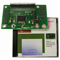
KIT33886DHEVB
Specifications of KIT33886DHEVB


Related parts for KIT33886DHEVB

KIT33886DHEVB Summary of contents
Page 1
... Temperature-Dependent Threshold Reduction) • Output Short-circuit Protection • Under-voltage Shutdown • Fault Status Reporting Freescale Semiconductor, Inc. reserves the right to change the detail specifications, as may be required, to permit improvements in the design of its products. © Freescale Semiconductor, Inc., 2007 - 2011. All rights reserved. MC33886PVW/R2 5 ...
Page 2
... INTERNAL BLOCK DIAGRAM CCP C CP Charge Charge Pump Pump Current Limit, Current Limit, Short-circuit Sense Circuit Gate Drive Gate Drive Over- Over- temperature temperature Under-voltage Undervoltage V+ V PWR Overcurrent Sense Circuit OUT1 OUT2 PGND Analog Integrated Circuit Device Data Freescale Semiconductor ...
Page 3
... PGND Power Ground 13 D2 Disable 2 14, 15 OUT2 H-Bridge Output 2 Charge Pump Capacitor External reservoir capacitor connection for internal charge pump capacitor. 17 CCP 18 D1 Disable 1 19 IN2 Logic Input Control 2 Analog Integrated Circuit Device Data Freescale Semiconductor PIN CONNECTIONS AGND IN1 OUT1 ...
Page 4
... ZAP = 200 pF, R ZAP Value Unit 40 V -0.1 to 7.0 V 7 ±2000 ±200 °C -65 to 150 °C -40 to 125 °C -40 to 150 °C Note 7. °C/W ~5.0 = 1500 Ω). ZAP = 0 Ω). ZAP (junction-to-PC board) θ JB Analog Integrated Circuit Device Data Freescale Semiconductor ...
Page 5
... Refer to typical operating curves to extrapolate values for operation > but ≤ 11. Inputs IN1, IN2, and D1 have independent internal pull-up current sources. 12. The D2 input incorporates an active internal pull-down current sink. Analog Integrated Circuit Device Data Freescale Semiconductor 125 °C, unless otherwise noted. Typical values noted ≤ V+ ≤ and -40°C ≤ ...
Page 6
... A 5.2 6.5 7 – – A 8.0 – – μA – 100 200 – – – 2.0 °C 175 – – – 15 – μA – – – – 1.0 Analog Integrated Circuit Device Data Freescale Semiconductor ...
Page 7
... C will cause the active current limiting to progressively “fold-back” (or decrease) to 2.5 A typical at 175 latch-OFF will occur. See Figure 7, page 8. Analog Integrated Circuit Device Data Freescale Semiconductor 125 °C, unless otherwise noted. Typical values noted ≤ V+ ≤ and -40°C ≤ ...
Page 8
... Figure 7. Active Current Limiting Versus Temperature (Typical) 33886 8 TIMING DIAGRAMS 50% 50 d(OFF) d(ON) 90% TIME Figure 4. Output Delay Time Figure 5. Disable Delay Time t f 90% 10% 10% Figure 6. Output Switching Time 160 175 JUNCTION TEMPERATURE ( C) 10 90% Thermal Shutdown Analog Integrated Circuit Device Data Freescale Semiconductor ...
Page 9
... Outputs Outputs Tristated Tri-stated [0] Figure 8. Active Current Limiting Versus Time 8.0 6.5 Analog Integrated Circuit Device Data Freescale Semiconductor Diode Reverse Recovery Spikes Load Capacitance and/or Diode Reverse Recovery Spikes PWM Active Current Current Hard Short Detect and Latch-OFF Limiting ...
Page 10
... OUT Input Voltage (IN1) Figure 13. Output Voltage and Current vs. Input Voltage PMW Frequency of 1.0 kHz, Duty Cycle=50% V+= =1.0 kHz Duty Cycle=90% PWM Current Limiting Mode V+= =1.0 kHz Duty Cycle=90% PWM and Duty Cycle of 90% Analog Integrated Circuit Device Data Freescale Semiconductor ...
Page 11
... V+= =10 kHz PWM Figure 15. Output Voltage and Current vs. Input Voltage PMW Frequency of 10 kHz, and Duty Cycle of 90% Analog Integrated Circuit Device Data Freescale Semiconductor Output Voltage (OUT1) I OUT Input Voltage (IN1) Duty Cycle=50% Figure 16. Output Voltage and Current vs. Input Voltage ...
Page 12
... When a short-circuit or over-temperature condition is detected, the power outputs are tri-state latched-OFF independent of the input signals and the fault status flag is set logic Low. 33886 The truth table uses the following notations Low, Input Conditions D1 D2 IN1 IN2 Fault Status Output States Flag FS OUT1 OUT2 Analog Integrated Circuit Device Data Freescale Semiconductor ...
Page 13
... Figure 18. Typical High Side R 0.13 0.128 0.126 0.124 0.122 0. Figure 19. Typical Low Side R Analog Integrated Circuit Device Data Freescale Semiconductor ELECTRICAL PERFORMANCE CURVES Volts Versus V+ DS(ON Volts V PWR Versus V+ DS(ON) ELECTRICAL CHARACTERISTICS ELECTRICAL PERFORMANCE CURVES ...
Page 14
... ELECTRICAL CHARACTERISTICS ELECTRICAL PERFORMANCE CURVES 9.0 8.0 7.0 6.0 5.0 4.0 3.0 2.0 1.0 0 Figure 20. Typical Quiescent Supply Current Versus V+ 33886 Volts V PWR Analog Integrated Circuit Device Data Freescale Semiconductor ...
Page 15
... High. Analog Integrated Circuit Device Data Freescale Semiconductor FUNCTIONAL DESCRIPTION INTRODUCTION external pull-up resistor is required for the open drain FS pin for fault status reporting. ...
Page 16
... PGND. The device C CP can operate without the external capacitor, although the capacitor helps to reduce noise and allows the device to perform at maximum speed, timing, and PWM frequency. Analog Integrated Circuit Device Data Freescale Semiconductor C CP ...
Page 17
... LIM Figure 7, page 8). This feature allows the device to remain Analog Integrated Circuit Device Data Freescale Semiconductor operational for a longer time but at a regressing output performance level at junction temperatures above 160 °C. OVER-TEMPERATURE SHUTDOWN AND HYSTERESIS If an over-temperature condition occurs, the power outputs are tri-state (latched-OFF) independent of the input signals and the fault status flag is set logic Low ...
Page 18
... PCB described in 100 2 10 Rth (¬¨ÐóC 1 0,1 0,001 0,01 Figure 22. 33886 Thermal Response Bottom Side Figure 21. 0 100 1000 10000 t, Time (s) Analog Integrated Circuit Device Data Freescale Semiconductor ...
Page 19
... A typical application schematic is shown in precision high-current applications in harsh, noisy IN2 IN1 Figure 23. 33886 Typical Application Schematic Analog Integrated Circuit Device Data Freescale Semiconductor TYPICAL APPLICATIONS Figure 23. For environments, the V+ by-pass capacitor may need to be substantially larger. DC MOTOR 33886 AGND V+ CCP OUT2 ...
Page 20
... PACKAGING PACKAGE DIMENSIONS Important For the most current revision of the package, visit 33886 20 PACKAGING PACKAGE DIMENSIONS www.freescale.com and perform a keyword search on 98ASH70702A listed. VW (Pb-FREE) SUFFIX 20-PIN HSOP 98ASH70702A ISSUE B Analog Integrated Circuit Device Data Freescale Semiconductor ...
Page 21
... Analog Integrated Circuit Device Data Freescale Semiconductor VW (Pb-FREE) SUFFIX 20-PIN HSOP 98ASH70702A ISSUE B PACKAGING PACKAGE DIMENSIONS 33886 21 ...
Page 22
... PACKAGING PACKAGE DIMENSIONS 33886 22 VW (Pb-FREE) SUFFIX 20-PIN HSOP 98ASH70702A ISSUE B Analog Integrated Circuit Device Data Freescale Semiconductor ...
Page 23
... JEDEC JESD51-3 and JESD51-5. 5.Thermal resistance between the die junction and the exposed pad surface; cold plate attached to the package bottom side, remaining surfaces insulated. Analog Integrated Circuit Device Data Freescale Semiconductor ), and thermal J P [°C/ ...
Page 24
... R is the thermal resistance between die junction and the θ JS reference location on the board surface near a center lead of the package (see Figure 25 2 °C/W Area A (mm ) 0.0 52 300 36 600 32 0.0 10 300 7.0 600 6.0 ). Analog Integrated Circuit Device Data Freescale Semiconductor ...
Page 25
... Figure 26. Device on Thermal Test Board R 100 10 1 0.1 1.00E-03 1.00E-02 1.00E-01 1.00E+00 1.00E+01 1.00E+02 1.00E+03 1.00E+04 Device on Thermal Test Board Area A = 600 (mm Analog Integrated Circuit Device Data Freescale Semiconductor x R θJA 0 300 Heat spreading area A [mm² θJA Time(s) Figure 27. Transient Thermal Resistance R 5 ...
Page 26
... Removed part number MC33886VW/R2 and added part number MC33886PVW/R2 to the ordering 3/2011 9.0 Information on page 1. • Updated package drawing. • Removed all DH package information. • Updated fom and style 33886 26 REVISION HISTORY DESCRIPTION OF CHANGES 4. Added note with instructions to obtain this information from Analog Integrated Circuit Device Data Freescale Semiconductor ...
Page 27
... Freescale Semiconductor product could create a situation where personal injury or death may occur. Should Buyer ...