EVAL-AD7661CB Analog Devices Inc, EVAL-AD7661CB Datasheet - Page 21
EVAL-AD7661CB
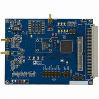
Manufacturer Part Number
EVAL-AD7661CB
Description
BOARD EVAL FOR AD7661
Manufacturer
Analog Devices Inc
Series
PulSAR®r
Datasheet
1.AD7661ACPZRL.pdf
(28 pages)
Specifications of EVAL-AD7661CB
Number Of Adc's
1
Number Of Bits
16
Sampling Rate (per Second)
100k
Data Interface
Serial, Parallel
Inputs Per Adc
1 Differential
Input Range
±VREF
Power (typ) @ Conditions
16mW @ 100kSPS
Voltage Supply Source
Analog and Digital
Operating Temperature
-40°C ~ 85°C
Utilized Ic / Part
AD7661
Lead Free Status / RoHS Status
Contains lead / RoHS non-compliant


CONVERSION CONTROL
Figure 33 shows the detailed timing diagrams of the conversion
process. The AD7661 is controlled by the CNVST signal, which
initiates conversion. Once initiated, it cannot be restarted or
aborted, even by the power-down input PD, until the conversion
is complete. CNVST operates independently of CS and RD .
Conversions can be automatically initiated with the AD7661. If
CNVST is held LOW when BUSY is LOW, the AD7661 controls
the acquisition phase and automatically initiates a new
conversion. By keeping CNVST LOW, the AD7661 keeps the
conversion process running by itself. It should be noted that the
analog input must be settled when BUSY goes LOW. Also, at
power-up, CNVST should be brought LOW once to initiate the
conversion process. In this mode, the AD7661 can run slightly
faster than the guaranteed 100 kSPS.
Although CNVST is a digital signal, it should be designed with
special care with fast, clean edges, and levels with minimum
overshoot and undershoot or ringing.
The CNVST trace should be shielded with ground and a low
value serial resistor (i.e., 50 Ω) termination should be added
close to the output of the component that drives this line.
For applications where SNR is critical, the CNVST signal should
have very low jitter. This may be achieved by using a dedicated
oscillator for CNVST generation, or to clock CNVST with a
high frequency, low jitter clock, as shown in Figure 26.
Rev. 0 | Page 21 of 28
CS = RD = 0
MODE
CNVST
CNVST
BUSY
RESET
CNVST
BUSY
BUSY
DATA
DATA
BUS
Figure 35. Master Parallel Data Timing for Reading (Continuous Read)
ACQUIRE
t
t
3
5
t
3
t
Figure 33. Basic Conversion Timing
PREVIOUS CONVERSION DATA
CONVERT
1
t
7
Figure 34. RESET Timing
t
4
t
t
1
9
t
2
t
6
t
10
ACQUIRE
t
t
4
8
t
8
t
11
AD7661
NEW DATA
CONVERT
Related parts for EVAL-AD7661CB
Image
Part Number
Description
Manufacturer
Datasheet
Request
R

Part Number:
Description:
ENERCHIP CC EVAL KIT
Manufacturer:
Cymbet Corporation
Datasheet:

Part Number:
Description:
BOARD EVAL FOR AD976
Manufacturer:
Analog Devices Inc
Datasheet:

Part Number:
Description:
BOARD EVAL FOR ADXL345
Manufacturer:
Analog Devices Inc
Datasheet:

Part Number:
Description:
ENERCHIP CC SEH EVAL KIT
Manufacturer:
Cymbet Corporation
Datasheet:

Part Number:
Description:
ENERCHIP EP ENERGY HARVEST EVAL
Manufacturer:
Cymbet Corporation
Datasheet:

Part Number:
Description:
EVAL BOARD FOR TW6864-LB2-GR
Manufacturer:
Intersil
Datasheet:
Part Number:
Description:
EVAL BOARD FOR TW8816-LB3-GR
Manufacturer:
Intersil
Datasheet:
Part Number:
Description:
EVAL BOARD FOR TW8817-TA3-GRS
Manufacturer:
Intersil
Datasheet:

Part Number:
Description:
EVALUATION MODULE FOR ADUM4160
Manufacturer:
Analog Devices Inc
Datasheet:

Part Number:
Description:
BOARD EVALUATION ADCMP581BCP
Manufacturer:
Analog Devices Inc
Datasheet:
Part Number:
Description:
BOARD EVALUATION ADM1041
Manufacturer:
Analog Devices Inc
Datasheet:

Part Number:
Description:
EVAL BOARD FOR STM32F107VCT
Manufacturer:
STMicroelectronics
Datasheet:
Part Number:
Description:
BOARD EVAL FOR AD1954
Manufacturer:
Analog Devices Inc
Datasheet:
Part Number:
Description:
BOARD EVAL FOR AD1955
Manufacturer:
Analog Devices Inc
Datasheet:

Part Number:
Description:
BOARD EVAL FOR AD7655
Manufacturer:
Analog Devices Inc
Datasheet: