EVAL-AD7864-1CB Analog Devices Inc, EVAL-AD7864-1CB Datasheet - Page 16
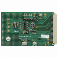
EVAL-AD7864-1CB
Manufacturer Part Number
EVAL-AD7864-1CB
Description
BOARD EVAL FOR AD7864-1
Manufacturer
Analog Devices Inc
Datasheet
1.AD7864ASZ-1.pdf
(28 pages)
Specifications of EVAL-AD7864-1CB
Number Of Adc's
1
Number Of Bits
12
Sampling Rate (per Second)
520k
Data Interface
Parallel
Inputs Per Adc
4 Differential
Input Range
±10 V
Power (typ) @ Conditions
90mW @ 520kSPS
Voltage Supply Source
Analog and Digital
Operating Temperature
-40°C ~ 85°C
Utilized Ic / Part
AD7864-1
Lead Free Status / RoHS Status
Contains lead / RoHS non-compliant


AD7864
logic high). The pointer is incremented to point to the next
register (next conversion result) when that conversion result is
available. Thus, FRSTDATA in Figure 9 is shown as going low
just prior to the second EOC pulse. Repeated read operations
during a conversion continue to access the data at the current
pointer location until the pointer is incremented at the end of
that conversion. Note that FRSTDATA has an indeterminate
logic state after initial power-up. This means that for the first
conversion sequence after power-up, the FRSTDATA logic
output may already be logic high before the end of the first
conversion (this condition is indicated by the dashed line in
Figure 9
high as a result of the previous read sequence, as is the case after
the fourth read in
resets the pointer to the first data location. Therefore, FRSTDATA
). Also, the FRSTDATA logic output may already be
Figure 9
SL1 TO SL4
FRSTDATA
FRSTDATA
CONVST
CONVST
H/S SEL
BUSY
DATA
BUSY
DATA
EOC
EOC
. The fourth read (rising edge of
RD
CS
RD
CS
t
2
t
2
t
1
t
1
t
CONV
t
3
Figure 10. Timing Diagram, Reading After the Conversion Sequence
100ns
100ns
t
BUSY
Figure 9. Timing Diagram for Reading During Conversion
t
8
V
t
12
IN1
t
t
10
CONV
t
6
t
4
V
RD)
IN1
Rev. D | Page 16 of 28
t
6
t
BUSY
t
t
11
V
5
IN2
V
IN2
t
t
3
3
t
8
t
CONV
t
t
is already high when the next conversion sequence initiates. See
the
Reading After the Conversion Sequence
Figure 10 shows the same conversion sequence as Figure 9. In
this case, however, the results of the four conversions (on V
V
BUSY goes logic low. The FRSTDATA signal goes logic high at
the end of the first conversion just prior to EOC going logic low.
As mentioned previously, FRSTDATA has an indeterminate
state after initial power-up, therefore FRSTDATA may already
be logic high. Unlike the case when reading between each
conversion, the output data register pointer is incremented on
the rising edge of RD because the next conversion result is
available. This means FRSTDATA goes logic low after the first
rising edge on RD.
7
7
IN4
V
IN3
Accessing the Output Data Registers
) are read after all conversions have finished, that is, when
V
t
4
IN3
V
IN4
t
CONV
t
10
QUIET
TIME
V
IN4
V
IN1
t
ACQ
QUIET
TIME
t
10
section.
IN1
to
Related parts for EVAL-AD7864-1CB
Image
Part Number
Description
Manufacturer
Datasheet
Request
R


Part Number:
Description:
BOARD EVAL FOR SI270X-A
Manufacturer:
Silicon Laboratories Inc
Datasheet:

Part Number:
Description:
BUCK CONV REF DESIGN KIT IP1201
Manufacturer:
International Rectifier
Datasheet:
Part Number:
Description:
BOARD DEMO SYNC DUAL BUCK CNVTER
Manufacturer:
International Rectifier
Datasheet:
Part Number:
Description:
BOARD DEMO SYNC BUCK CONVETER
Manufacturer:
International Rectifier
Datasheet:

Part Number:
Description:
EVALBOARD/EB Omnidirectional microphone - Analog
Manufacturer:
Analog Devices
Datasheet:
Part Number:
Description:
EVALBOARD/EB Omnidirectional microphone - Analog
Manufacturer:
Analog Devices
Datasheet:


Part Number:
Description:
BOARD EVAL LED DRIVER LT3756
Manufacturer:
Linear Technology
Datasheet:

Part Number:
Description:
BOARD EVAL FOR AD7741/7742
Manufacturer:
Analog Devices Inc
Datasheet:

Part Number:
Description:
±1.7g Dual-Axis IMEMS Accelerometer Evaluation Board
Manufacturer:
Analog Devices Inc
Datasheet:

Part Number:
Description:
IC MULTIPLIER ANALOG 8-SOIC T/R
Manufacturer:
Analog Devices Inc
Datasheet:

Part Number:
Description:
IC ANALOG MULTIPLIER 8-DIP
Manufacturer:
Analog Devices Inc
Datasheet:
Part Number:
Description:
IC ANALOG MULTIPLIER 8-SOIC
Manufacturer:
Analog Devices Inc
Datasheet:
Part Number:
Description:
IC ANALOG MULTIPLIER 8-DIP
Manufacturer:
Analog Devices Inc
Datasheet: