EVAL-AD7864-1CB Analog Devices Inc, EVAL-AD7864-1CB Datasheet
EVAL-AD7864-1CB
Specifications of EVAL-AD7864-1CB


Related parts for EVAL-AD7864-1CB


EVAL-AD7864-1CB Summary of contents
Page 1
FEATURES High speed (1.65 μs) 12-bit ADC 4 simultaneously sampled inputs 4 track-and-hold amplifiers 0.35 μs track-and-hold acquisition time 1.65 μs conversion time per channel HW/SW select of channel sequence for conversion Single-supply operation Selection of input ranges ±10 V, ...
Page 2
AD7864 TABLE OF CONTENTS Features .............................................................................................. 1 Applications ....................................................................................... 1 General Description ......................................................................... 1 Functional Block Diagram .............................................................. 1 Product Highlights ........................................................................... 1 Revision History ............................................................................... 2 Specifications ..................................................................................... 3 Timing Characteristics ................................................................ 5 Absolute Maximum Ratings ............................................................ 6 ESD ...
Page 3
SPECIFICATIONS ± 5%, AGND = DGND = Table 1. Parameter SAMPLE AND HOLD −3 dB Full Power Bandwidth Aperture Delay Aperture Jitter Aperture Delay Matching 2 DYNAMIC PERFORMANCE 3 Signal-to-(Noise + Distortion) ...
Page 4
AD7864 Parameter AD7864-2 Input Voltage Range Input Current ( 2.5 V Option) Input Resistance ( Option) REFERENCE INPUT/OUTPUT V In Input Voltage Range REF Input Capacitance REF V Out Output Voltage ...
Page 5
TIMING CHARACTERISTICS V± 5%, AGND = DGND = DRIVE Table 2. Parameter A, B Versions t 1.65 CONV 13 2.6 t 0.34 ACQ t No. of channels × BUSY ( CONV 9 ...
Page 6
AD7864 ABSOLUTE MAXIMUM RATINGS T = 25°C, unless otherwise noted. A Table 3. Parameter AV to AGND DGND DD AGND to DGND Analog Input Voltage to AGND AD7864-1 (±10 V Input Range) ...
Page 7
PIN CONFIGURATION AND FUNCTION DESCRIPTIONS FRSTDAT Table 4. Pin Function Descriptions Pin No. Mnemonic Description 1 BUSY Busy Output. The busy output is triggered high by the rising edge of CONVST and remains high until conversion is completed on all ...
Page 8
AD7864 Pin No. Mnemonic Description 27 INT /EXT CLK Internal/External Clock Select Input. When this pin is at Logic 0, the AD7864 uses its internally generated master clock. When this pin is at Logic 1, the master clock is generated ...
Page 9
TERMINOLOGY Signal-to-(Noise + Distortion) Ratio This is the measured ratio of signal-to-(noise + distortion) at the output of the ADC. The signal is the rms amplitude of the fundamental. Noise is the rms sum of all nonfundamental signals up to ...
Page 10
AD7864 It means that the user must wait for the duration of the track- and-hold acquisition time after the end of conversion or after a step input change before starting another INxA INxB conversion to ensure that ...
Page 11
THEORY OF OPERATION CONVERTER DETAILS The AD7864 is a high speed, low power, 4-channel simultaneous sampling 12-bit ADC that operates from a single 5 V supply. The part contains a 1.65 μs successive approximation ADC, four track-and-hold amplifiers, an internal ...
Page 12
AD7864 nominal source impedance for this output. The tolerance on the internal reference is ± 25°C with a typical temperature coefficient of 25 ppm/°C and a maximum error overtemperature of ±20 mV. If the application requires a reference ...
Page 13
CIRCUIT DESCRIPTION ANALOG INPUT The AD7864 is offered in three models: the AD7864-1, where each input can be configured for ± ±5 V input voltage range; the AD7864-3, which handles the input voltage range of ±2.5 V; ...
Page 14
AD7864 Table 6. Ideal Input/Output Code Table for the AD7864-2 Analog Input 1 Digital Output Code Transition 2 +FSR − 3/2 LSB 111...110 to 111...111 +FSR − 5/2 LSB 111...101 to 111...110 +FSR − 7/2 LSB 111...100 to 111...101 AGND ...
Page 15
SELECTING A CONVERSION SEQUENCE Any subset of the four channels IN1 conversion. The selected channels are converted in ascending order. For example, if the channel selection includes V and V , the conversion sequence is V IN3 ...
Page 16
AD7864 logic high). The pointer is incremented to point to the next register (next conversion result) when that conversion result is available. Thus, FRSTDATA in Figure 9 is shown as going low just prior to the second EOC pulse. Repeated ...
Page 17
Successive read operations access the remaining conversion results in an ascending channel order. Each read operation increments the output data register pointer. The read operation that accesses the last conversion result causes the output data register pointer to be reset ...
Page 18
AD7864 STANDBY MODE OPERATION The AD7864 has a standby mode whereby the device can be placed in a low current consumption mode (5 μA typical). The AD7864 is placed in standby by bringing the Logic Input STBY low. The AD7864 ...
Page 19
When reading the output data registers after a conversion sequence, that is, when BUSY goes low, the register pointer is incremented on the rising edge of the RD signal, as shown in Figure 14 . However, when reading the conversion ...
Page 20
AD7864 OFFSET AND FULL-SCALE ADJUSTMENT In most digital signal processing (DSP) applications, offset and full-scale errors have little or no effect on system performance. Offset error can always be eliminated in the analog domain by ac coupling. Full-scale error effect ...
Page 21
... ADC CODE Figure 16. Histogram of 8192 Conversions Input The output spectrum from the ADC is evaluated by applying a sine wave signal of very low distortion to the analog input. A fast fourier transform (FFT) plot is generated from which the SNR data can be obtained. Figure 17 shows a typical 4096 point FFT plot of the AD7864 with an input signal of 99 ...
Page 22
AD7864 terms include (fa + fb) and (fa − fb), whereas the third-order terms include (2fa + fb), (2fa − fb), (fa + 2fb), and (fa − 2fb). Using the CCIF standard where two input frequencies near the top end ...
Page 23
From Figure 22, the ENOB of the AD7864 at 1 MHz is approximately 11 bits. This is equivalent SNR. SNR = SNR + SNR = 68 dB TOTAL JITTER QUANT SNR + 72 dB ...
Page 24
AD7864 MICROPROCESSOR INTERFACING The high speed parallel interface of the AD7864 allows easy interfacing to most DSPs and microprocessors. This interface consists of the data lines (DB0 to DB11), CS, RD, WR, EOC, and BUSY. AD7864 TO ADSP-2100/ADSP-2101/ADSP-2102 INTERFACE Figure ...
Page 25
ADDRESS DECODE V CS IN1 V IN2 V IN3 RD V IN4 AD7864 DB0 TO DB11 CLOCK CONVST Figure 25. AD7864 to MC68HC000 Interface VECTOR MOTOR CONTROL The current drawn by a motor can be split into two components: one ...
Page 26
AD7864 MULTIPLE AD7864S IN A SYSTEM Figure 27 shows a system where a number of AD7864s are configured to handle multiple input channels. This type of configuration is common in applications such as sonar and radar. The AD7864 is specified ...
Page 27
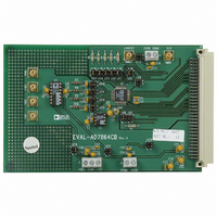
... This board is a complete unit, allowing control and communicate with all Analog Devices, Inc., evaluation boards ending in the CB designators. To order a complete evaluation kit, the particular ADC evaluation board needs to be ordered, for example, EVAL-AD7864-1CB, the EVAL-CONTROL BRD2, and transformer. See the Evaluation Board application note for more information. ...
Page 28
AD7864 NOTES ©1998–2009 Analog Devices, Inc. All rights reserved. Trademarks and registered trademarks are the property of their respective owners. D01341-0-2/09(D) Rev Page ...