EVAL-AD7856CB Analog Devices Inc, EVAL-AD7856CB Datasheet - Page 7
EVAL-AD7856CB
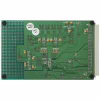
Manufacturer Part Number
EVAL-AD7856CB
Description
BOARD EVAL FOR AD7856
Manufacturer
Analog Devices Inc
Datasheet
1.AD7856ARSZ-REEL7.pdf
(32 pages)
Specifications of EVAL-AD7856CB
Lead Free Status / RoHS Status
Contains lead / RoHS non-compliant


REV. A
Pin
1
2
3
4
5
6
7
8
9–16
17
18
19
20
21
22
23
24
Mnemonic
CONVST
BUSY
SLEEP
REF
AV
AGND
C
C
AIN1–AIN8
CAL
DV
DGND
DOUT
DIN
CLKIN
SCLK
SYNC
REF1
REF2
DD
DD
IN
/REF
OUT
Description
Convert Start. Logic Input. A low to high transition on this input puts the track/hold into its hold mode
and starts conversion. When this input is not used, it should be tied to DV
Busy Output. The busy output is triggered high by the falling edge of CONVST or rising edge of CAL,
and remains high until conversion is completed. BUSY is also used to indicate when the AD7856 has
completed its on-chip calibration sequence.
Sleep Input/Low Power Mode. A Logic 0 initiates a sleep, and all circuitry is powered down, including
the internal voltage reference, provided there is no conversion or calibration being performed. Calibration
data is retained. A Logic 1 results in normal operation. See Power-Down section for more details.
Reference Input/Output. This pin is connected to the internal reference through a series resistor and is
the reference source for the analog-to-digital converter. The nominal reference voltage is 4.096 V and
this appears at the pin. This pin can be overdriven by an external reference or can be taken as high as
AV
C
Analog Positive Supply Voltage, +5.0 V
Analog Ground. Ground reference for track/hold, reference and DAC.
Reference Capacitor (0.1 F Multilayer Ceramic in parallel with a 470 nF NPO type). This external
capacitor is used as a charge source for the internal DAC. The capacitor should be tied between the pin
and AGND.
Reference Capacitor (0.01 F Multilayer Ceramic). This external capacitor is used in conjunction with
the on-chip reference. The capacitor should be tied between the pin and AGND.
Analog Inputs. Eight analog inputs that can be used as eight single-ended inputs (referenced to AGND)
or four pseudo-differential inputs. Channel configuration is selected by writing to the control register.
Both the positive and negative inputs cannot go below AGND or above AV
tive input cannot go below the negative input. See Table III for channel selection.
Calibration Input. This pin has an internal pull-up current source of 0.15 A. A falling edge on this pin
resets all calibration control logic and initiates a calibration on its rising edge. There is the option of
connecting a 10 nF capacitor from this pin to DGND to allow for an automatic self-calibration on
power-up. This input overrides all other internal operations. If the autocalibration is not required, this
pin should be tied to a logic high.
Digital Supply Voltage, +5.0 V
Digital Ground. Ground reference point for digital circuitry.
Serial Data Output. The data output is supplied to this pin as a 16-bit serial word.
Serial Data Input. The data to be written is applied to this pin in serial form (16-bit word). This pin can
act as an input pin or as a I/O pin depending on the serial interface mode the part is in (see Table X).
Master clock signal for the device (A Grade: 6 MHz; K Grade: 4 MHz). Sets the conversion and calibra-
tion times.
Serial Port Clock. Logic Input. The user must provide a serial clock on this input.
Frame Sync. Logic Input. This pin is level triggered active low and frames the serial clock for the read
and write operations (see Table IX).
REF1
DD
. When this pin is tied to AV
pin should also be tied to AV
PIN FUNCTION DESCRIPTIONS
5%.
DD
DD,
–7–
.
or when an externally applied reference approaches AV
5%.
DD
DD
.
at any time. Also the posi-
AD7856
DD,
the
Related parts for EVAL-AD7856CB
Image
Part Number
Description
Manufacturer
Datasheet
Request
R

Part Number:
Description:
ENERCHIP CC EVAL KIT
Manufacturer:
Cymbet Corporation
Datasheet:

Part Number:
Description:
BOARD EVAL FOR AD976
Manufacturer:
Analog Devices Inc
Datasheet:

Part Number:
Description:
BOARD EVAL FOR ADXL345
Manufacturer:
Analog Devices Inc
Datasheet:

Part Number:
Description:
ENERCHIP CC SEH EVAL KIT
Manufacturer:
Cymbet Corporation
Datasheet:

Part Number:
Description:
ENERCHIP EP ENERGY HARVEST EVAL
Manufacturer:
Cymbet Corporation
Datasheet:

Part Number:
Description:
EVAL BOARD FOR TW6864-LB2-GR
Manufacturer:
Intersil
Datasheet:
Part Number:
Description:
EVAL BOARD FOR TW8816-LB3-GR
Manufacturer:
Intersil
Datasheet:
Part Number:
Description:
EVAL BOARD FOR TW8817-TA3-GRS
Manufacturer:
Intersil
Datasheet:

Part Number:
Description:
EVALUATION MODULE FOR ADUM4160
Manufacturer:
Analog Devices Inc
Datasheet:

Part Number:
Description:
BOARD EVALUATION ADCMP581BCP
Manufacturer:
Analog Devices Inc
Datasheet:
Part Number:
Description:
BOARD EVALUATION ADM1041
Manufacturer:
Analog Devices Inc
Datasheet:

Part Number:
Description:
EVAL BOARD FOR STM32F107VCT
Manufacturer:
STMicroelectronics
Datasheet:
Part Number:
Description:
BOARD EVAL FOR AD1954
Manufacturer:
Analog Devices Inc
Datasheet:
Part Number:
Description:
BOARD EVAL FOR AD1955
Manufacturer:
Analog Devices Inc
Datasheet:

Part Number:
Description:
BOARD EVAL FOR AD7655
Manufacturer:
Analog Devices Inc
Datasheet: