EVAL-AD7655CB Analog Devices Inc, EVAL-AD7655CB Datasheet - Page 19
EVAL-AD7655CB
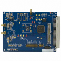
Manufacturer Part Number
EVAL-AD7655CB
Description
BOARD EVAL FOR AD7655
Manufacturer
Analog Devices Inc
Series
PulSAR®r
Specifications of EVAL-AD7655CB
Number Of Adc's
1
Number Of Bits
16
Sampling Rate (per Second)
1M
Data Interface
Serial, Parallel
Inputs Per Adc
4 Single Ended
Input Range
0 ~ 2 V
Power (typ) @ Conditions
120mW @ 1MSPS
Voltage Supply Source
Analog and Digital
Operating Temperature
-40°C ~ 85°C
Utilized Ic / Part
AD7655
Lead Free Status / RoHS Status
Contains lead / RoHS non-compliant


Slave Parallel Interface
In slave parallel reading mode, the data can be read either after
each conversion, which is during the next acquisition phase, or
during the other channel’s conversion, or during the following
conversion, as shown in Figure 24 and Figure 25, respectively.
When the data is read during the conversion, however, it is
recommended that it is read only during the first half of the
conversion phase. This avoids any potential feedthrough
between voltage transients on the digital interface and the most
critical analog conversion circuitry.
CNVST, RD
DATA BUS
Figure 25. Slave Parallel Data Timing for Reading (Read During Convert)
DATA BUS
Figure 24. Slave Parallel Data Timing for Reading (Read after Convert)
CS
BUSY
EOC
BUSY
= 0
RD
CS
t
t
t
18
10
3
t
18
CONVERSION
PREVIOUS
t
1
CONVERSION
CURRENT
t
t
19
11
t
19
t
4
t
12
t
13
Rev. B | Page 19 of 28
8-Bit Interface (Master or Slave)
The BYTESWAP pin allows a glueless interface to an 8-bit bus.
As shown in Figure 26, the LSB byte is output on D[7:0] and the
MSB is output on D[15:8] when BYTESWAP is low. When
BYTESWAP is high, the LSB and MSB bytes are swapped, the
LSB is output on D[15:8], and the MSB is output on D[7:0]. By
connecting BYTESWAP to an address line, the 16-bit data can
be read in 2 bytes on either D[15:8] or D[7:0].
Channel A/ B Output
The A/ B input controls which channel’s conversion results
(INAx or INBx) are output on the data bus. The function-ality
of A/ B is detailed in Figure 27. When high, the data from
Channel A is available on the data bus. When low, the data from
Channel B is available on the bus. Note that in parallel reading
mode, Channel A can be read immediately after the end of
conversion ( EOC ), while Channel B is still in its converting
phase. However, in any of the serial reading modes Channel A
data is updated only after Channel B conversion.
DATA BUS
PINS D[15:8]
BYTESWAP
PINS D[7:0]
A/B
CS
RD
CS
RD
HI-Z
HI-Z
HI-Z
Figure 26. 8-Bit Parallel Interface
Figure 27. A/ B Channel Reading
t
18
CHANNEL A
t
18
HIGH BYTE
LOW BYTE
t
20
CHANNEL B
t
18
HIGH BYTE
LOW BYTE
AD7655
HI-Z
HI-Z
HI-Z
t
19
Related parts for EVAL-AD7655CB
Image
Part Number
Description
Manufacturer
Datasheet
Request
R

Part Number:
Description:
ENERCHIP CC EVAL KIT
Manufacturer:
Cymbet Corporation
Datasheet:

Part Number:
Description:
BOARD EVAL FOR AD976
Manufacturer:
Analog Devices Inc
Datasheet:

Part Number:
Description:
BOARD EVAL FOR ADXL345
Manufacturer:
Analog Devices Inc
Datasheet:

Part Number:
Description:
ENERCHIP CC SEH EVAL KIT
Manufacturer:
Cymbet Corporation
Datasheet:

Part Number:
Description:
ENERCHIP EP ENERGY HARVEST EVAL
Manufacturer:
Cymbet Corporation
Datasheet:

Part Number:
Description:
EVAL BOARD FOR TW6864-LB2-GR
Manufacturer:
Intersil
Datasheet:
Part Number:
Description:
EVAL BOARD FOR TW8816-LB3-GR
Manufacturer:
Intersil
Datasheet:
Part Number:
Description:
EVAL BOARD FOR TW8817-TA3-GRS
Manufacturer:
Intersil
Datasheet:

Part Number:
Description:
EVALUATION MODULE FOR ADUM4160
Manufacturer:
Analog Devices Inc
Datasheet:

Part Number:
Description:
BOARD EVALUATION ADCMP581BCP
Manufacturer:
Analog Devices Inc
Datasheet:
Part Number:
Description:
BOARD EVALUATION ADM1041
Manufacturer:
Analog Devices Inc
Datasheet:

Part Number:
Description:
EVAL BOARD FOR STM32F107VCT
Manufacturer:
STMicroelectronics
Datasheet:
Part Number:
Description:
BOARD EVAL FOR AD1954
Manufacturer:
Analog Devices Inc
Datasheet:
Part Number:
Description:
BOARD EVAL FOR AD1955
Manufacturer:
Analog Devices Inc
Datasheet:

Part Number:
Description:
BOARD EVAL FOR AD9831
Manufacturer:
Analog Devices Inc
Datasheet: