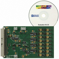
EVAL-AD7490CB Analog Devices Inc, EVAL-AD7490CB Datasheet - Page 19
EVAL-AD7490CB
Manufacturer Part Number
EVAL-AD7490CB
Description
BOARD EVAL FOR AD7490
Manufacturer
Analog Devices Inc
Datasheet
1.AD7490BRUZ.pdf
(28 pages)
Specifications of EVAL-AD7490CB
Number Of Adc's
1
Number Of Bits
12
Sampling Rate (per Second)
1M
Data Interface
Serial
Inputs Per Adc
16 Single Ended
Input Range
0 ~ 5 V
Power (typ) @ Conditions
12.5mW @ 1MSPS, 5 V
Voltage Supply Source
Single
Operating Temperature
-40°C ~ 85°C
Utilized Ic / Part
AD7490
Lead Free Status / RoHS Status
Contains lead / RoHS non-compliant


Reference Section
An external reference source should be used to supply the 2.5 V
reference to the AD7490. Errors in the reference source result
in gain errors in the AD7490 transfer function and add to the
specified full-scale errors of the part. A capacitor of at least 0.1 μF
should be placed on the REF
for the AD7490 include the AD780, REF192, AD1582, ADR03,
ADR381, ADR391, and ADR421.
If 2.5 V is applied to the REF
either be 0 V to 2.5 V or 0 V to 5 V, depending on the RANGE
bit in the control register.
MODES OF OPERATION
The AD7490 has a number of different modes of operation.
These modes are designed to provide flexible power manage-
ment options. These options can be chosen to optimize the
power dissipation/throughput rate ratio for differing application
requirements. The mode of operation of the AD7490 is controlled
by the power management bits, PM1 and PM0, in the control
register, as detailed in Table 7. When power supplies are first
applied to the AD7490, care should be taken to ensure that the
part is placed in the required mode of operation (see the
Powering Up the AD7490 section).
Normal Mode (PM1 = PM0 = 1)
This mode is intended for the fastest throughput rate performance
because the user does not have to worry about any power-up
times with the AD7490 remaining fully powered at all times.
Figure 22 shows the general diagram of the operation of the
AD7490 in this mode.
DOUT
NOTES
1. CONTROL REGISTER DATA IS LOADED ON FIRST 12 SCLK CYCLES
2. SHADOW REGISTER DATA IS LOADED ON FIRST 16 SCLK CYCLES
SCLK
DIN
CS
CHANNE L IDENTIFIER BITS + CONVERSION RESULT
DATA IN TO CONTROL/SHADOW REGISTER
1
Figure 22. Normal Mode Operation
DOUT
SCLK
DIN
CS
PART IS IN FULL
SHUTDOWN
IN
IN
pin. Suitable reference sources
pin, the analog input range can
CONTROL REGISTER IS LOADED ON THE
FIRST 12 CLOCKS, PM1 = 1, PM0 = 1
1
DATA IN TO CONTROL REGISTER
12
PART BEGINS TO POWER UP ON CS
RISING EDGE AS PM1 = 1, PM0 = 1
16
Figure 23. Full Shutdown Mode Operation
14
Rev. C | Page 19 of 28
16
PART IS FULLY POWERED UP
ONCE
CHANNE L IDENTIFIER BITS + CONVERSION RESULT
The conversion is initiated on the falling edge of CS , and the
track-and-hold enters hold mode, as described in the
Interface
DIN line during the first 12 clock cycles of the data transfer is
loaded
to the control register (provided the WRITE bit is 1). If data is
to be written to the Shadow register (SEQ = 0, SHADOW = 1
on previous write), data presented on the DIN line during the
first 16 SCLK cycles is loaded into the Shadow register. The part
remains fully powered up in normal mode at the end of the
conversion as long as PM1 and PM0 are set to 1 in the write
transfer during that conversion. To ensure continued operation
in normal mode, PM1 and PM0 are both loaded with 1 on every
data transfer. Sixteen serial clock cycles are required to complete
the conversion and access the conversion result. The track-and-
hold goes back into track on the 14
then idle high until the next conversion or may idle low until
sometime prior to the next conversion, (effectively idling CS low).
Once a data transfer is complete (DOUT has returned to three-
state WEAK/ TRI bit = 0), another conversion can be initiated
after the quiet time, t
Full Shutdown (PM1 = 1, PM0 = 0)
In this mode, all internal circuitry on the AD7490 is powered
down. The part retains information in the control register
during full shutdown. The AD7490 remains in full shutdown
until the power management bits in the control register, PM1
and PM0, are changed.
If a write to the control register occurs while the part is in
full shutdown, with the power management bits changed to
PM0 = PM1 = 1 (normal mode), the part begins to power up
on the CS rising edge. The track-and-hold that was in hold
while the part was in full shutdown returns to track on the 14
SCLK falling edge.
To ensure that the part is fully powered up, t
elapse before the next CS falling edge.
general diagram for this mode.
DATA IN TO CONTROL/SHADOW REGISTER
TO KEEP PART IN NORMAL MODE, LOAD
PM1 = 1, PM0 = 1 IN CONTROL REGISTER
t
12
1
t
POWER UP
section. The data presented to the AD7490 on the
HAS ELAPSED
QUIET
, has elapsed by bringing CS low again.
14
16
th
SCLK falling edge. CS may
Figure 23
POWER UP
shows the
(t
AD7490
12
Serial
) should
th
Related parts for EVAL-AD7490CB
Image
Part Number
Description
Manufacturer
Datasheet
Request
R

Part Number:
Description:
ENERCHIP CC EVAL KIT
Manufacturer:
Cymbet Corporation
Datasheet:

Part Number:
Description:
BOARD EVAL FOR AD976
Manufacturer:
Analog Devices Inc
Datasheet:

Part Number:
Description:
BOARD EVAL FOR ADXL345
Manufacturer:
Analog Devices Inc
Datasheet:

Part Number:
Description:
ENERCHIP CC SEH EVAL KIT
Manufacturer:
Cymbet Corporation
Datasheet:

Part Number:
Description:
ENERCHIP EP ENERGY HARVEST EVAL
Manufacturer:
Cymbet Corporation
Datasheet:

Part Number:
Description:
EVAL BOARD FOR TW6864-LB2-GR
Manufacturer:
Intersil
Datasheet:
Part Number:
Description:
EVAL BOARD FOR TW8816-LB3-GR
Manufacturer:
Intersil
Datasheet:
Part Number:
Description:
EVAL BOARD FOR TW8817-TA3-GRS
Manufacturer:
Intersil
Datasheet:

Part Number:
Description:
EVALUATION MODULE FOR ADUM4160
Manufacturer:
Analog Devices Inc
Datasheet:

Part Number:
Description:
BOARD EVALUATION ADCMP581BCP
Manufacturer:
Analog Devices Inc
Datasheet:
Part Number:
Description:
BOARD EVALUATION ADM1041
Manufacturer:
Analog Devices Inc
Datasheet:

Part Number:
Description:
EVAL BOARD FOR STM32F107VCT
Manufacturer:
STMicroelectronics
Datasheet:
Part Number:
Description:
BOARD EVAL FOR AD1954
Manufacturer:
Analog Devices Inc
Datasheet:
Part Number:
Description:
BOARD EVAL FOR AD1955
Manufacturer:
Analog Devices Inc
Datasheet:

Part Number:
Description:
BOARD EVAL FOR AD7655
Manufacturer:
Analog Devices Inc
Datasheet: