AD8362-EVAL Analog Devices Inc, AD8362-EVAL Datasheet - Page 5
AD8362-EVAL
Manufacturer Part Number
AD8362-EVAL
Description
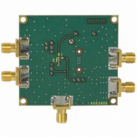
BOARD EVAL FOR AD8362
Manufacturer
Analog Devices Inc
Datasheet
1.AD8362-EVAL.pdf
(32 pages)
Specifications of AD8362-EVAL
Rohs Status
RoHS non-compliant


Parameter
2.7 GHz
3.65 GHz
1
2
3
4
1:4 balun transformer, M/A-COM ETC 1.6-4-2-3.
See Figure 48.
See Figure 50.
The limitation of the high end of the power range is due to the test equipment not the device under test.
Dynamic Range
Deviation vs. Temperature
Logarithmic Slope
Logarithmic Intercept
Deviation from CW Response
Dynamic Range
Deviation vs. Temperature
Logarithmic Slope
Logarithmic Intercept
Conditions
Error referred to best-fit line (linear regression)
±1.0 dB linearity, CW input
±0.5 dB linearity, CW input
Deviation from output at 25°C
−40°C < T
−40°C < T
−40°C < T
5.5 dB peak-to-rms ratio (IS95 reverse link)
12.0 dB peak-to-rms ratio (W-CDMA 4 channels)
18.0 dB peak-to-rms ratio (W-CDMA 15 channels)
Single-ended drive
Error referred to best-fit line (linear regression)
±1.0 dB linearity, CW input
±0.5 dB linearity, CW input
Deviation from output at 25°C
−40°C < T
−40°C < T
−40°C < T
A
A
A
A
A
A
< +85°C, P
< +85°C, P
< +85°C, P
< +85°C, P
< +85°C, P
< +85°C, P
3
IN
IN
IN
IN
IN
IN
= −40 dBm
= −15 dBm
= +5 dBm
= −35 dBm
= −15 dBm
= +10 dBm
Rev. D | Page 5 of 32
Min
Typ
63
62
−5.3
−5.5
−4.8
50.5
−58
0.2
0.2
0.4
51
50
−3
−3.5
−3.5
51.7
−45
Max
AD8362
Unit
dB
dB
dB
dB
dB
mV/dB
dBm
dB
dB
dB
dB
dB
dB
dB
dB
mV/dB
dBm
Related parts for AD8362-EVAL
Image
Part Number
Description
Manufacturer
Datasheet
Request
R

Part Number:
Description:
BOARD EVAL FOR AD8362
Manufacturer:
Analog Devices Inc
Datasheet:

Part Number:
Description:
±1.7g Dual-Axis IMEMS Accelerometer Evaluation Board
Manufacturer:
Analog Devices Inc
Datasheet:
Part Number:
Description:
Inertial Sensor Evaluation System
Manufacturer:
Analog Devices Inc
Datasheet:
Part Number:
Description:
Manufacturer:
Analog Devices Inc
Datasheet:
Part Number:
Description:
Manufacturer:
Analog Devices Inc
Datasheet:
Part Number:
Description:
Manufacturer:
Analog Devices Inc
Datasheet:
Part Number:
Description:
Manufacturer:
Analog Devices Inc
Datasheet:
Part Number:
Description:
Manufacturer:
Analog Devices Inc
Datasheet:
Part Number:
Description:
Manufacturer:
Analog Devices Inc
Datasheet:
Part Number:
Description:
Manufacturer:
Analog Devices Inc
Datasheet:
Part Number:
Description:
Manufacturer:
Analog Devices Inc
Datasheet:
Part Number:
Description:
Manufacturer:
Analog Devices Inc
Datasheet:
Part Number:
Description:
Manufacturer:
Analog Devices Inc
Datasheet: