AD8362-EVAL Analog Devices Inc, AD8362-EVAL Datasheet - Page 13
AD8362-EVAL
Manufacturer Part Number
AD8362-EVAL
Description
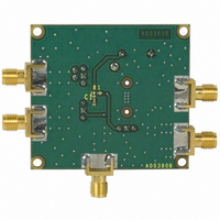
BOARD EVAL FOR AD8362
Manufacturer
Analog Devices Inc
Datasheet
1.AD8362-EVAL.pdf
(32 pages)
Specifications of AD8362-EVAL
Rohs Status
RoHS non-compliant


Figure 34. Output Response Using Power-Down Mode for Various RF Input
Figure 33. Output Response to RF Burst Input for Various RF Input Levels,
5.0
4.5
4.0
3.5
3.0
2.5
2.0
1.5
1.0
0.5
5.0
4.5
4.0
3.5
3.0
2.5
2.0
1.5
1.0
0.5
5.0
4.5
4.0
3.5
3.0
2.5
2.0
1.5
1.0
0.5
0
0
0
0
0
0
RF Input Levels, Carrier Frequency 900 MHz, CLPF = Open
Figure 32. Output Response to RF Burst Input for Various
2
2
2
Levels, Carrier Frequency 900 MHz, CLPF = 0
Carrier Frequency 900 MHz, CLPF = 0.1 μF
4
4
4
6
6
6
8
8
8
TIME (ms)
TIME (µs)
TIME (µs)
–10dBm
–20dBm
–30dBm
–10dBm
–20dBm
–30dBm
10
10
10
–10dBm
–20dBm
–30dBm
12
12
12
14
14
14
16
16
16
18
18
18
2
2
2
0
0
0
6
4
2
0
–2
–4
–6
–8
–10
–12
–14
6
4
2
0
–2
–4
–6
–8
–10
–12
–14
6
4
2
0
–2
–4
–6
–8
–10
–12
–14
Rev. D | Page 13 of 32
Figure 36. Output Response to Gating on Power Supply for Various RF Input
Figure 35. Output Response Using Power-Down Mode for Various RF Input
Figure 37. INHI, INLO Differential Input Impedance, 100 MHz to 3 GHz
5.0
4.5
4.0
3.5
3.0
2.5
2.0
1.5
1.0
0.5
5.5
5.0
4.5
4.0
3.5
3.0
2.5
2.0
1.5
1.0
0
0
0
0
2
2
Levels, Carrier Frequency 900 MHz, CLPF = 0.1 μF
Levels, Carrier Frequency 900 MHz, CLPF = 0
4
4
6
6
VPOS
8
8
TIME (ms)
TIME (ms)
–10dBm
–20dBm
–30dBm
10
10
100MHz
3GHz
12
12
14
14
–10dBm
–20dBm
–30dBm
16
16
18
18
AD8362
2
2
0
0
6
4
2
0
–2
–4
–6
–8
–10
–12
–14
6
4
2
0
–2
–4
–6
–8
–10
–12
–14
Related parts for AD8362-EVAL
Image
Part Number
Description
Manufacturer
Datasheet
Request
R

Part Number:
Description:
BOARD EVAL FOR AD8362
Manufacturer:
Analog Devices Inc
Datasheet:

Part Number:
Description:
±1.7g Dual-Axis IMEMS Accelerometer Evaluation Board
Manufacturer:
Analog Devices Inc
Datasheet:
Part Number:
Description:
Inertial Sensor Evaluation System
Manufacturer:
Analog Devices Inc
Datasheet:
Part Number:
Description:
Manufacturer:
Analog Devices Inc
Datasheet:
Part Number:
Description:
Manufacturer:
Analog Devices Inc
Datasheet:
Part Number:
Description:
Manufacturer:
Analog Devices Inc
Datasheet:
Part Number:
Description:
Manufacturer:
Analog Devices Inc
Datasheet:
Part Number:
Description:
Manufacturer:
Analog Devices Inc
Datasheet:
Part Number:
Description:
Manufacturer:
Analog Devices Inc
Datasheet:
Part Number:
Description:
Manufacturer:
Analog Devices Inc
Datasheet:
Part Number:
Description:
Manufacturer:
Analog Devices Inc
Datasheet:
Part Number:
Description:
Manufacturer:
Analog Devices Inc
Datasheet:
Part Number:
Description:
Manufacturer:
Analog Devices Inc
Datasheet: