AD8362-EVAL Analog Devices Inc, AD8362-EVAL Datasheet - Page 2
AD8362-EVAL
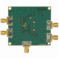
Manufacturer Part Number
AD8362-EVAL
Description
BOARD EVAL FOR AD8362
Manufacturer
Analog Devices Inc
Datasheet
1.AD8362-EVAL.pdf
(32 pages)
Specifications of AD8362-EVAL
Rohs Status
RoHS non-compliant


AD8362
TABLE OF CONTENTS
Features .............................................................................................. 1
Applications....................................................................................... 1
Functional Block Diagram .............................................................. 1
General Description ......................................................................... 1
Revision History ............................................................................... 2
Specifications..................................................................................... 3
Absolute Maximum Ratings............................................................ 6
Pin Configuration and Function Descriptions............................. 7
Equivalent Circuits ........................................................................... 8
Typical Performance Characteristics ............................................. 9
Characterization Setup .................................................................. 15
Circuit Description......................................................................... 16
REVISION HISTORY
6/07—Rev. C to Rev. D
Changes to Features, General Description.................................... 1
Changes to Table 1............................................................................ 3
Changes to Table 2............................................................................ 6
Added Figure 21 to Figure 25........................................................ 11
Changes to Equipment Section..................................................... 15
Changes to Circuit Description Section ...................................... 16
Changes to Single-Ended Input Drive Section ........................... 19
Changes to Choosing a Value for CHPF section........................ 21
Changes to Choosing a Value for CLPF section......................... 21
Changes to Figure 57...................................................................... 23
Changes to Figure 58...................................................................... 24
Added Temperature Compensation at Various WiMAX
Frequencies up to 3.8 GHz Section .............................................. 24
Changes to Ordering Guide .......................................................... 31
9/05—Rev. B to Rev. C
Changes to Specifications................................................................ 3
Changes to Table 3 ........................................................................... 7
Deleted Figure 16 to Figure 18; Renumbered Sequentially ...... 10
Changes to Figure 32 and Figure 33 ............................................ 13
ESD Caution.................................................................................. 6
Equipment ................................................................................... 15
Analysis........................................................................................ 15
Square Law Detection ................................................................ 16
Voltage vs. Power Calibration ................................................... 17
Offset Elimination...................................................................... 18
Time-Domain Response of the Closed Loop ......................... 18
Rev. D | Page 2 of 32
Operation in RF Measurement Mode.......................................... 19
Temperature Compensation at Various WiMAX Frequencies up
to 3.8 GHz........................................................................................ 24
AD8362 Evaluation Board ............................................................ 28
Outline Dimensions ....................................................................... 31
Replaced Circuit Description Section ......................................... 15
Changes to Operation in RF Measurement Mode Section ...... 18
Deleted Using the AD8362 Section ............................................. 20
Deleted Main Modes of Operation Section................................ 22
Changes to Operation in Controller Mode Section .................. 23
Changes to AD8362 Evaluation Board Section.......................... 25
Deleted General Applications Section......................................... 29
3/04—Rev. A to Rev. B
Updated Format .................................................................Universal
Changes to Specifications.................................................................3
Changes to the Offset Elimination Section................................. 16
Changes to the Operation at Low Frequencies Section ............ 17
Changes to the Time-Domain Response of the Closed
Loop Section.................................................................................... 17
Changes to Equation 13................................................................. 24
Changes to Table 5 ......................................................................... 31
6/03—Rev. 0 to Rev. A
Updated Ordering Guide .................................................................5
Change to Analysis Section........................................................... 12
Updated AD8362 Evaluation Board Section .............................. 26
2/03—Revision 0: Initial Version
Basic Connections...................................................................... 19
Device Disable ............................................................................ 19
Recommended Input Coupling................................................ 19
Operation at Low Frequencies.................................................. 20
Choosing a Value for CHPF...................................................... 21
Choosing a Value for CLPF....................................................... 21
Adjusting VTGT to Accommodate Signals with Very High
Crest Factors ............................................................................... 22
Altering the Slope....................................................................... 22
Temperature Compensation and Reduction of Transfer
Function Ripple .......................................................................... 23
Operation in Controller Mode ................................................. 26
RMS Voltmeter with 90 dB Dynamic Range .......................... 27
Ordering Guide .......................................................................... 31
Related parts for AD8362-EVAL
Image
Part Number
Description
Manufacturer
Datasheet
Request
R

Part Number:
Description:
BOARD EVAL FOR AD8362
Manufacturer:
Analog Devices Inc
Datasheet:

Part Number:
Description:
±1.7g Dual-Axis IMEMS Accelerometer Evaluation Board
Manufacturer:
Analog Devices Inc
Datasheet:
Part Number:
Description:
Inertial Sensor Evaluation System
Manufacturer:
Analog Devices Inc
Datasheet:
Part Number:
Description:
Manufacturer:
Analog Devices Inc
Datasheet:
Part Number:
Description:
Manufacturer:
Analog Devices Inc
Datasheet:
Part Number:
Description:
Manufacturer:
Analog Devices Inc
Datasheet:
Part Number:
Description:
Manufacturer:
Analog Devices Inc
Datasheet:
Part Number:
Description:
Manufacturer:
Analog Devices Inc
Datasheet:
Part Number:
Description:
Manufacturer:
Analog Devices Inc
Datasheet:
Part Number:
Description:
Manufacturer:
Analog Devices Inc
Datasheet:
Part Number:
Description:
Manufacturer:
Analog Devices Inc
Datasheet:
Part Number:
Description:
Manufacturer:
Analog Devices Inc
Datasheet:
Part Number:
Description:
Manufacturer:
Analog Devices Inc
Datasheet: