ECLSOIC8EVB ON Semiconductor, ECLSOIC8EVB Datasheet - Page 4
ECLSOIC8EVB
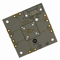
Manufacturer Part Number
ECLSOIC8EVB
Description
BOARD EVALUATION HI FREQ 8-SOIC
Manufacturer
ON Semiconductor
Datasheet
1.ECLSOIC8EVB.pdf
(20 pages)
Specifications of ECLSOIC8EVB
Main Purpose
Bare Evaluation Board
Lead Free Status / RoHS Status
Contains lead / RoHS non-compliant
Other names
ECLSOIC8EVB
ECLSOIC8EVBOS
ECLSOIC8EVBOS


characterizing devices in a 50 W laboratory environment
using high bandwidth equipment. Each signal trace on the
board has a via, which has an option of termination resistor
or bypassing capacitor depending on the input/output
configuration (see Table 1. Configuration List). Table 17
contains the Bill of Materials for this evaluation board.
Solder the Device on the Evaluation Board
soldering re−flow techniques. Make sure pin 1 of the device
is located next the white dotted mark U1 and all the pins are
aligned to the footprint pads. Solder the 8−lead SOIC device
to the evaluation board.
Connecting Power and Ground Planes
supply is required enabling the 50 W internal impedance in
the oscilloscope to be used as a termination of the ECL
signals (V
is the system ground, V
–1.3 V; see Table 2: Power Supply Levels).
The power supply for voltage level translating device need
slight modification as indicated in Table 3. Power Supply
Levels for Translators.
Table 2. Power Supply Levels
Table 3. Power Supply Levels for Translators
The 8−lead SOIC evaluation board is designed for
The soldering can be accomplished by hand soldering or
For standard ECL lab setup and test, a split (dual) power
Power Supply
PECL Translators
Evaluation Board Assembly Instructions
5.0 V
3.3 V
2.5 V
TT
= V
CC
– 2.0 V, in split power supply setup, V
2.0 V
2.0 V
2.0 V
V
CC
CC
3.3 V / 5.0 V
is 2.0 V, and V
V
CC
−3.0 V
−1.3 V
−0.5 V
V
EE
0.0 V
V
EE
EE
is –3.0 V or
0.0 V
0.0 V
0.0 V
GND
0.0 V
GND
http://onsemi.com
ECLSOIC8EVB
TT
4
surface mount test point clips to the pads labeled V
and GND. The V
device. The V
There are two GND clip footprints which can be connected
to the ground plane of the evaluation board depending on the
setup configuration.
C2 to reduce the unwanted noise from the power supplies.
C3 and C4 pads are provided for 0.1 mF capacitor to further
diminish the noise from the power supplies. Adding
capacitors can improve edge rates, reduce overshoot and
undershoot.
Termination
–2.0 V = GND) via a 50 W resistor in a split power supply
lab set−up. 0603 chip resistor pads are provided on the
bottom side of the evaluation board to terminate the ECL
driver (More information on termination is provided in
AN8020). Solder the chip resistors to the bottom side of the
board on the appropriate input of the device pins labeled R1,
R2, R3, R4, R6, and R7, depending on the specific device.
Installing the SMA Connectors
connectors needed to populate an evaluation board for a
given configuration. Each input and output requires one
SMA connector. Attach all the required SMA connectors
onto the board and solder the connectors to the board. Please
note that alignment of the signal connector pin of the SMA
can influence the lab results. The reflection and launch of the
signals are largely influenced by imperfect alignment and
soldering of the SMA connector.
Validating the Assembled Board
to perform continuity checks on all soldered areas before
commencing with the evaluation process. Time Domain
Reflectometry (TDR) is another highly recommended
validation test.
On the top side of the evaluation board solder the four
It is recommended to solder 0.01 mF capacitors to C1 and
All ECL outputs need to be terminated to V
Each configuration indicates the number of SMA
After assembling the evaluation board, it is recommended
EE
clip connects directly to pin 5 of the device.
CC
clip connects directly to pin 8 of the
TT
(V
TT
CC
= V
, V
EE
CC
,
Related parts for ECLSOIC8EVB
Image
Part Number
Description
Manufacturer
Datasheet
Request
R

Part Number:
Description:
ON Semiconductor [VOLTAGE REGULATOR]
Manufacturer:
ON Semiconductor
Datasheet:
Part Number:
Description:
357-036-542-201 CARDEDGE 36POS DL .156 BLK LOPRO
Manufacturer:
ON Semiconductor
Datasheet:
Part Number:
Description:
357-036-542-201 CARDEDGE 36POS DL .156 BLK LOPRO
Manufacturer:
ON Semiconductor
Datasheet:
Part Number:
Description:
357-036-542-201 CARDEDGE 36POS DL .156 BLK LOPRO
Manufacturer:
ON Semiconductor
Datasheet:
Part Number:
Description:
357-036-542-201 CARDEDGE 36POS DL .156 BLK LOPRO
Manufacturer:
ON Semiconductor
Datasheet:
Part Number:
Description:
357-036-542-201 CARDEDGE 36POS DL .156 BLK LOPRO
Manufacturer:
ON Semiconductor
Datasheet:
Part Number:
Description:
357-036-542-201 CARDEDGE 36POS DL .156 BLK LOPRO
Manufacturer:
ON Semiconductor
Datasheet:
Part Number:
Description:
357-036-542-201 CARDEDGE 36POS DL .156 BLK LOPRO
Manufacturer:
ON Semiconductor
Datasheet:
Part Number:
Description:
357-036-542-201 CARDEDGE 36POS DL .156 BLK LOPRO
Manufacturer:
ON Semiconductor
Datasheet:
Part Number:
Description:
357-036-542-201 CARDEDGE 36POS DL .156 BLK LOPRO
Manufacturer:
ON Semiconductor
Datasheet:
Part Number:
Description:
357-036-542-201 CARDEDGE 36POS DL .156 BLK LOPRO
Manufacturer:
ON Semiconductor
Datasheet:
Part Number:
Description:
Manufacturer:
ON Semiconductor
Datasheet:
Part Number:
Description:
Manufacturer:
ON Semiconductor
Datasheet:
Part Number:
Description:
Manufacturer:
ON Semiconductor
Datasheet: