XCARD XTAG-2 XMOS, XCARD XTAG-2 Datasheet - Page 6
XCARD XTAG-2
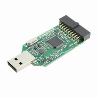
Manufacturer Part Number
XCARD XTAG-2
Description
ADAPTER USB DEBUGGER JTAG XSYS2
Manufacturer
XMOS
Type
In Circuit Debuggerr
Specifications of XCARD XTAG-2
Design Resources
XTAG-2 Schematic
Contents
Board
For Use With/related Products
XMOS Development Boards
Lead Free Status / RoHS Status
Lead free / RoHS Compliant


XTAG-2 Hardware Manual (1.0)
4.2 XMOS Link Configuration
Some of the I/O pins on the processor are configured as a duplex 2-bit serial XMOS
Link. The mapping of XMOS Link to the pins is shown in the table below:
4.3 JTAG Configuration
Some of the I/O pins on the processor are driven by the JTAG signals. The mapping
of the signals to the pins is shown in the table below:
4.4 System Reset
The system reset signal is mapped to a 1-bit port on the processor as described
below. It is used as an output to reset the target processor from the debugger
5 13MHz Crystal Oscillator
The XS1-L1 is clocked at 13MHz by a crystal oscillator on the card. The processor is
clocked at 400MHz and the I/O ports at 100MHz, by an on-chip phaselocked loop
(PLL).
Pin
XD0
XD1
XD10 P1C0 TMS
XD11 P1D0 TCK
XD35 P1L0
Pin
XD36 P1IM RST_N
www.xmos.com
Pin
XD4 XL1_UP1
XD5 XL1_UP0
XD6 XL1_DN0
XD7 XL1_DN1
Port
P1A0 TDSRC
P1B0
Port
XMOS Link
Processor
Processor
TDSNK
TRST_N
6/8
Related parts for XCARD XTAG-2
Image
Part Number
Description
Manufacturer
Datasheet
Request
R

Part Number:
Description:
BOARD DEV KIT XS1-G4 ETHERNET
Manufacturer:
XMOS
Datasheet:

Part Number:
Description:
BOARD DEV KIT XS1-G4
Manufacturer:
XMOS
Datasheet:

Part Number:
Description:
DEV KIT EVENT-DRIVEN PROC XS1-L1
Manufacturer:
XMOS
Datasheet:

Part Number:
Description:
BOARD KIT XS1-G4 LED CTRL TILE
Manufacturer:
XMOS
Datasheet:

Part Number:
Description:
BOARD DEV KIT XS1-G4
Manufacturer:
XMOS
Datasheet:

Part Number:
Description:
IC MPU 32BIT SINGLE CORE 64LQFP
Manufacturer:
XMOS
Datasheet:

Part Number:
Description:
IC MPU 32BIT SINGLE CORE 64LQFP
Manufacturer:
XMOS
Datasheet:
Part Number:
Description:
IC MPU 32BIT SINGLE CORE 64LQFP
Manufacturer:
XMOS
Datasheet:

Part Number:
Description:
IC MPU 32BIT SINGLE CORE 64LQFP
Manufacturer:
XMOS
Datasheet:
Part Number:
Description:
IC MPU 32BIT SINGLE CORE 64LQFP
Manufacturer:
XMOS
Datasheet:

Part Number:
Description:
IC MPU 32BIT SINGLE CORE 128TQFP
Manufacturer:
XMOS
Datasheet:
Part Number:
Description:
IC MPU 32BIT SINGLE CORE 64LQFP
Manufacturer:
XMOS
Datasheet:
Part Number:
Description:
IC MPU 32BIT SINGLE CORE 128TQFP
Manufacturer:
XMOS
Datasheet:
Part Number:
Description:
IC MPU 32BIT SINGLE CORE 128TQFP
Manufacturer:
XMOS
Datasheet:

Part Number:
Description:
IC MPU 32BIT DUAL CORE 124QFN
Manufacturer:
XMOS
Datasheet: