XCARD XTAG-2 XMOS, XCARD XTAG-2 Datasheet
XCARD XTAG-2
Specifications of XCARD XTAG-2


Related parts for XCARD XTAG-2


XCARD XTAG-2 Summary of contents
Page 1
... XTAG-2 Hardware Manual Publication Date: 2009/09/23 Copyright © 2009 XMOS Ltd. All Rights Reserved. Version 1.0 ...
Page 2
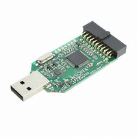
... The diagram below shows the layout of the components on the card. 20-way IDC XSYS Connector To debug a board with the XTAG-2 you must use the XMOS Design Tools version 9.9 or later, available from the 2 XS1-L1 Device The XTAG-2 is based on a single XS1-L1 device in a 64LQFP package. The XS1-L1 consists of a single XCore, which comprises an event-driven multi-threaded processor with tightly integrated general purpose I/O pins and 64 KBytes of on-chip RAM ...
Page 3
... The reset pin on the USB transceiver is mapped to a 1-bit port on the processor as described below: Standard-A type USB Connector USB Transceiver (USB3318) Port Processor 4bit 8bit ULPI_STP ULPI_NXT ULPI_DATA[0:7] ULPI_DIR ULPI_CLK Pin Port Processor XD24 P1I0 PHY_RST_N www.xmos.com 3/8 ...
Page 4
... XSYS Connector The XTAG-2 includes an XSYS 20-way IDC header, which can be used to connect XMOS development board for debugging programs on the hardware. The XSYS connector provides pins for JTAG control, system reset, processor debug, a duplex UART link and a 2-bit serial XMOS Link. ...
Page 5
... The table below shows the pin-to-port mapping TRST_N GND TDSRC XL1_UP1 TMS GND TCK XL1_UP0 DEBUG GND TDSNK XL1_DN0 RST_N GND UART_RX XL1_DN1 UART_TX GND 19 20 UART_RX UART_TX Pin Port Processor 1bit 4bit XD25 P1J0 UART_RX XD26 P4E0 UART_TX www.xmos.com 5/8 ...
Page 6
... XTAG-2 Hardware Manual (1.0) 4.2 XMOS Link Configuration Some of the I/O pins on the processor are configured as a duplex 2-bit serial XMOS Link. The mapping of XMOS Link to the pins is shown in the table below: 4.3 JTAG Configuration Some of the I/O pins on the processor are driven by the JTAG signals. The mapping of the signals to the pins is shown in the table below: 4 ...
Page 7
... P8A5 XL1_DN1 P4A2 P8A6 P4A3 P8A7 TMS TCK ULPI_STP ULPI_NXT P4C0 P8B0 P4C1 P8B1 P4D0 P8B2 P4D1 P8B3 ULPI_DATA[0:7] P4D2 P8B4 P4D3 P8B5 P4C2 P8B6 P4C3 P8B7 ULPI_DIR ULPI_CLK PHY_RST_N UART_RX P4E0 UART_TX P4E1 P4E2 P4E3 DEBUG TRST_N RST_N www.xmos.com 7/8 ...
Page 8
... XMOS Ltd. is the owner or licensee of this design, code, or Information (collectively, the “Information”) and is providing it to you “AS IS” with no warranty of any kind, express or implied and shall have no liability in relation to its use. XMOS Ltd. makes no representation that the Information, or any particular implementation thereof will be free from any claims of infringement and again, shall have no liability in relation to any such claims ...