HW-V5-ML507-UNI-G Xilinx Inc, HW-V5-ML507-UNI-G Datasheet - Page 32
HW-V5-ML507-UNI-G
Manufacturer Part Number
HW-V5-ML507-UNI-G
Description
EVAL PLATFORM V5 FXT
Manufacturer
Xilinx Inc
Series
Virtex™-5 FXTr
Type
FPGAr
Datasheet
1.HW-V5-ML507-UNI-G.pdf
(60 pages)
Specifications of HW-V5-ML507-UNI-G
Contents
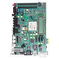
ML507 Platform, DVI adapter, CompactFlash Card and SATA Cross-Over Cable
Silicon Manufacturer
Xilinx
Features
JTAG Programming Interface, Platform Flash, External Clocking
Kit Contents
Board
Silicon Family Name
Virtex-5
Silicon Core Number
XC5VFX70TFFG1136
Lead Free Status / RoHS Status
Lead free / RoHS Compliant
For Use With/related Products
ML507
Lead Free Status / RoHS Status
Lead free / RoHS Compliant, Lead free / RoHS Compliant
Available stocks
Company
Part Number
Manufacturer
Quantity
Price


Chapter 1: ML505/ML506/ML507 Evaluation Platform
32
22. USB Controller with Host and Peripheral Ports
23. Xilinx XCF32P Platform Flash PROM Configuration Storage Devices
Note: J56 = SATA Clock Select
J22
J23
J24
GMII/MII to copper
J56
Jumpers J22, J23, and J24 allow the user to select the default interface that the PHY uses
(Figure 1-4
Table 1-16: PHY Default Interface Mode
A Cypress CY7C67300 embedded USB host controller provides USB connectivity for the
board. The USB controller supports host and peripheral modes of operation. The USB
controller has two serial interface engines (SIE) that can be used independently. SIE1 is
connected to the USB Host connector (P18). SIE2 is connected only to the USB Peripheral
connector (P17).
The USB controller has an internal microprocessor to assist in processing USB commands.
The firmware for this processor can be stored in its own dedicated IIC EEPROM (U28) or
can be downloaded from a host computer via a peripheral connector. The USB controller's
serial port is connected to J30 through an RS-232 transceiver to assist with debug. Jumper
J50 can be installed to prevent the USB controller from executing firmware stored in the IIC
EEPROM.
The two onboard Xilinx XCF32P Platform Flash PROM configuration storage devices offer
a convenient and easy-to-use configuration solution for the FPGA. The Platform Flash
PROM holds up to two separate configuration images (up to four with compression) that
can be accessed through the configuration address switches. To use the Platform Flash
PROM to configure the FPGA, the configuration DIP switch must be set to the correct
position.
GMII/MII to copper
SGMII to copper,
(default)
no clock
RGMII
Mode
and
Figure 1-4: PHY Jumpers on the Board
Table
J22
J23
J24
SGMII to copper; no clock
1-16). The interface can also be changed via MDIO commands.
www.xilinx.com
Jumper over pins 1-2
Jumper over pins 2-3
Jumper over pins 1-2
J56
J22
RGMII; modified MII in copper
Jumper Settings
ML505/ML506/ML507 Evaluation Platform
Jumper over pins 1-2
Jumper over pins 2-3
J22
J23
J24
No jumper
J23
UG347 (v3.1.1) October 7, 2009
J56
UG347_05_112706
No jumper
No jumper
Jumper on
J24
R
Related parts for HW-V5-ML507-UNI-G
Image
Part Number
Description
Manufacturer
Datasheet
Request
R

Part Number:
Description:
IC CPLD .8K 36MCELL 44-VQFP
Manufacturer:
Xilinx Inc
Datasheet:

Part Number:
Description:
IC CPLD 72MCRCELL 10NS 44VQFP
Manufacturer:
Xilinx Inc
Datasheet:

Part Number:
Description:
IC CPLD 1.6K 72MCELL 64-VQFP
Manufacturer:
Xilinx Inc
Datasheet:

Part Number:
Description:
IC CR-II CPLD 64MCELL 44-VQFP
Manufacturer:
Xilinx Inc
Datasheet:

Part Number:
Description:
IC CPLD 1.6K 72MCELL 100-TQFP
Manufacturer:
Xilinx Inc
Datasheet:

Part Number:
Description:
IC CR-II CPLD 64MCELL 56-BGA
Manufacturer:
Xilinx Inc
Datasheet:

Part Number:
Description:
IC CPLD 72MCRCELL 7.5NS 44VQFP
Manufacturer:
Xilinx Inc
Datasheet:
Part Number:
Description:
IC CR-II CPLD 64MCELL 100-VQFP
Manufacturer:
Xilinx Inc
Datasheet:
Part Number:
Description:
IC CPLD 1.6K 72MCELL 100-TQFP
Manufacturer:
Xilinx Inc
Datasheet:

Part Number:
Description:
IC CPLD 72MCRCELL 7.5NS 64VQFP
Manufacturer:
Xilinx Inc
Datasheet:
Part Number:
Description:
IC CPLD 1.6K 72MCELL 100-TQFP
Manufacturer:
Xilinx Inc
Datasheet:

Part Number:
Description:
IC CPLD 1.5K 64MCELL HP 44-VQFP
Manufacturer:
Xilinx Inc

Part Number:
Description:
IC CPLD 36MCRCELL 15NS 44PLCC
Manufacturer:
Xilinx Inc
Datasheet:

Part Number:
Description:
IC CPLD 36MCRCELL 10NS 44PLCC
Manufacturer:
Xilinx Inc
Datasheet:

Part Number:
Description:
IC CPLD 1.5K 64MCELL HP 44-VQFP
Manufacturer:
Xilinx Inc