EDK7145 Renesas Electronics America, EDK7145 Datasheet - Page 11
EDK7145
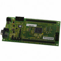
Manufacturer Part Number
EDK7145
Description
DEV EVALUATION KIT SH7145
Manufacturer
Renesas Electronics America
Type
MCUr
Datasheets
1.EDK7145.pdf
(19 pages)
2.EDK7145.pdf
(4 pages)
3.EDK7145.pdf
(5 pages)
4.EDK7145.pdf
(22 pages)
Specifications of EDK7145
Contents
2G (Second-generation) Evaluation Board, HEW debugger support, Cable and CD-ROM
Lead Free Status / RoHS Status
Contains lead / RoHS non-compliant
For Use With/related Products
SH7145
Lead Free Status / RoHS Status
Not Compliant, Contains lead / RoHS non-compliant


The SRAM is mapped to area 0 via chip select 0 (port PA10), with a usable address range of H’00200000 – H’0027FFFF
using address signals A1 – A18.
Glue logic provides the required SRAM control signals from the SH2/7145 micon.
4.4. M
Table 4-5 illustrates the EDK memory map for mode 2.
4.5. SRAM A
External access timing is defined by several registers, allowing different types of devices to be addressed. The registers for
the selection of wait states and signal extensions are given below with recommended values for the EDK.
Please refer to the hardware manual for the microcontroller for more information on these register settings.
4.6. LED
The EDK has four red LEDs. The function of each LED is marked on the silk screen of the PCB. Please refer to the board
layout diagram for position information (Figure 3.1).
When the board is connected to a power source the Power (PWR) LED will illuminate. The Boot mode indication LED will
illuminate when the microcontroller has been placed into Boot mode. Please see section 5.7 for more details of this function.
There are two LEDs dedicated for user control these are marked USR1 and USR2. Each LED will illuminate when the port
pin is in a logical high state.
The user LEDs are connected to the following ports:
(2 BITS)BCR2.IW0
(BIT)BCR1.A0SZ
EMORY
PACRL1
PDCRL1
PDCRL2
Register
PBCR2
S
PCCR
M
CCESS
AP
H’00000000
H’0003FFFF
H’00040000
H’001FFFFF
H’00200000
H’003FFFFF
H’00400000
H’00FFFFFF
H’01000000
H’FFFF7FFF
H’FFFF8000
H’FFFFBFFF
H’FFFFC000
H’FFFFDFFF
H’FFFFE000
H’FFFFFFFF
Identifier
T
USR1
USR2
LED
IMING
Setting for EDK
Recommended
0xFFFE
0xFFFF
0x1510
0x2005
0x0000
1
1
Section Start
Section End
PE14
PE15
Port
Pin
T
Enable CS0 (PA10), WRL (PA12), WRH (PA13), RD (PA14)
Enable A15 (PB0), A16 (PB1), A17 (PB6)
Enable D0 – D15 (PD0 – PD15) – Register 2 of 2 for Data Bus
CS1 accessed as word
1 Idle Cycle on CS1
Enable A1 – A15 (PC1 – PC15)
Enable D0 – D15 (PD0 – PD15) – Register 1 of 2 for Data Bus
ABLE
T
Microcontroller
ABLE
T
4-6: SRAM A
ABLE
4-5: M
Pin
2
5
4-7: LED P
EMORY
CCESS
On-chip ROM
Reserved Area
CS0
External Address Space
Reserved Area
Internal IO Registers
Reserved Area
On-Chip RAM (8kB)
M
ORT
AP
PE15/TIOC4D/DACK1/IRQOUTn
(512kB External RAM H’00200000 to
C
(D
C
ONTROL
EFAULT
ONNECTIONS
Pin Functions on Port Pin
PE14/TIOC4C/DACK0
Section Allocation
R
M
EGISTERS
ODE
Function
6)
H’0027FFFF)
8
Related parts for EDK7145
Image
Part Number
Description
Manufacturer
Datasheet
Request
R

Part Number:
Description:
KIT STARTER FOR M16C/29
Manufacturer:
Renesas Electronics America
Datasheet:

Part Number:
Description:
KIT STARTER FOR R8C/2D
Manufacturer:
Renesas Electronics America
Datasheet:

Part Number:
Description:
R0K33062P STARTER KIT
Manufacturer:
Renesas Electronics America
Datasheet:

Part Number:
Description:
KIT STARTER FOR R8C/23 E8A
Manufacturer:
Renesas Electronics America
Datasheet:

Part Number:
Description:
KIT STARTER FOR R8C/25
Manufacturer:
Renesas Electronics America
Datasheet:

Part Number:
Description:
KIT STARTER H8S2456 SHARPE DSPLY
Manufacturer:
Renesas Electronics America
Datasheet:

Part Number:
Description:
KIT STARTER FOR R8C38C
Manufacturer:
Renesas Electronics America
Datasheet:

Part Number:
Description:
KIT STARTER FOR R8C35C
Manufacturer:
Renesas Electronics America
Datasheet:

Part Number:
Description:
KIT STARTER FOR R8CL3AC+LCD APPS
Manufacturer:
Renesas Electronics America
Datasheet:
Part Number:
Description:
KIT STARTER FOR RX610
Manufacturer:
Renesas Electronics America
Datasheet:

Part Number:
Description:
KIT STARTER FOR R32C/118
Manufacturer:
Renesas Electronics America
Datasheet:

Part Number:
Description:
KIT DEV RSK-R8C/26-29
Manufacturer:
Renesas Electronics America
Datasheet:

Part Number:
Description:
KIT STARTER FOR SH7124
Manufacturer:
Renesas Electronics America
Datasheet:

Part Number:
Description:
KIT STARTER FOR H8SX/1622
Manufacturer:
Renesas Electronics America
Datasheet:

Part Number:
Description:
KIT DEV FOR SH7203
Manufacturer:
Renesas Electronics America
Datasheet: