EDK7145 Renesas Electronics America, EDK7145 Datasheet
EDK7145
Specifications of EDK7145


Related parts for EDK7145


EDK7145 Summary of contents
Page 1
To our customers, Old Company Name in Catalogs and Other Documents st On April 1 , 2010, NEC Electronics Corporation merged with Renesas Technology Corporation, and Renesas Electronics Corporation took over all the business of both companies. Therefore, although the ...
Page 2
All information included in this document is current as of the date this document is issued. Such information, however, is subject to change without any prior notice. Before purchasing or using any Renesas Electronics products listed herein, please confirm ...
Page 3
...
Page 4
... EDK7145 U M SER ANUAL F SH2/7145 FLASH M N CHIP ICROCONTROLLER ...
Page 5
Preface Cautions 1. This document may be, wholly or partially, subject to change without notice. 2. All rights reserved. No one is permitted to reproduce or duplicate, in any form, a part or this entire document without Hitachi Micro Systems ...
Page 6
T C ABLE OF ONTENTS ............................................................................................................................................. 3 ABLE OF ONTENTS ....................................................................................................................................... 4 TART UP NSTRUCTIONS 2.1. INSTALLING THE EVALUATION DEVELOPMENT KIT (EDK)........................................................................... 4 2.2. SERIAL CONNECTION ....................................................................................................................................... 4 2.3. POWER SUPPLY ................................................................................................................................................ ...
Page 7
TART UP NSTRUCTIONS 2. NSTALLING THE VALUATION Please refer to the quick start guide provided for initial installation of the EDK. A copy of the quick start guide and other information relating to this ...
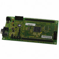
Page 8
EDK B L OARD AYOUT The diagram shows a general layout of the EDK board. FLASH Programming Power NMI Switch BOOT LED Power LED User1 LED User2 LED RESET BOOT Switch Switch CJ5 9-Way D-Type CJ4 3.1. EDK B ...
Page 9
EDK O PERATION 4.1. USER INTERFACE The EDK provides three buttons for influencing the operation of the board. The purpose of each button is clearly marked next to it. Refer to the board layout for positions (Figure 3.1) 1. ...
Page 10
C C RYSTAL HOICE The operating crystal frequency has been chosen to support the fastest operation with the fastest serial operating speeds. The value of the crystal is 11.0592MHz. The following table shows the baud rates and Baud Rate ...
Page 11
The SRAM is mapped to area 0 via chip select 0 (port PA10), with a usable address range of H’00200000 – H’0027FFFF using address signals A1 – A18. Glue logic provides the required SRAM control signals from the SH2/7145 micon. ...
Page 12
B O OARD PTIONS The EDK has a number of configuration settings set by jumpers CJ4 ( D), CJ5 ( and zero-ohm links. Common EDK functions can be set using the jumpers as described ...
Page 13
The default settings indicated in bold text place the microcontroller into operating Mode 3, i.e. on-chip ROM enabled, single chip mode and clock mode 3: System clock = x4, Peripheral clock = x2. 5.3. EDK O – CJ4 PTIONS The ...
Page 14
To enable the use of this alternate port the user must change the settings to those in the following table. Zero-ohm Default Link ID CR20 Not Fitted CR23 Not Fitted CR19 Fitted CR22 Fitted The user may implement a handshaking ...
Page 15
During user mode the NMI button can be pressed at any time. This will provide a single de-bounced NMI interrupt to the device. Pressing the boot button will cause the boot mode controller to reset the device and, during the ...
Page 16
M H ICROCONTROLLER EADER The following table lists the connections to each or the headers on the board. 6. EADER Pin Function EDK Symbol No 1 PD2/D2 3 PD4/D4 5 PD5/D5 7 PD6/D6 9 PD8/D8 11 PD10/D10 ...
Page 17
H J2 EADER Pin Function EDK Symbol No 1 PD1/D1 3 VSS GND 5 MD3 7 MD2 9 FWP FW 11 PA17/WAITn 13 MD0 PLLCAP (NO 15 CONNECTION) 17 PA15/CK PE0/TIOC0A/DREQ0 n/AUDCK 19 CON_PE0 PE2/TIOC0C/DREQ1 21 n/AUDRSTn PE3/TIOC0D/DRAK1 23 ...
Page 18
C D ODE EVELOPMENT 7.1. HMON HMON is an on-chip debugger from HMSE. It allows code to be debugged in Flash and/or RAM on their target hardware using the MCU’s debug capabilities. It consists of HMON components for HEW ...
Page 19
M M EMORY AP H'00000000 Vectors H'00001000 FDTInit H'0000113F H'00003000 PHMON CHMON H'00004F83 H'00007000 CUser_Vectors H'00007003 On-Chip FLASH ROM H'0003F800 FDTUserMode MicroKernel H'0003FFAF H'0003FFFF H'00200000 SRAM H'0027FFFF H'FFFF8000 Internal I/O REGISTERS H'FFFFBFFF H'FFFFE000 On-Chip RAM H'FFFFF400 BHMON H'FFFFF659 H'FFFFFBF0 ...
Page 20
AUD ATE ETTING HMON has initially set to connect at 115200Baud. Should the user wish to change this, the value for the BRR in HMONserialconfiguser.c will need to be changed and the project re-built. Please refer ...
Page 21
If we examine the actual opcodes being stepped, we can see the PC ...
Page 22
This opcode still reflects the source line LED_PORT_DR ^= LED_BIT and this is illustrated in the source window, as shown below in Figure 7-5. The CPU peforms 2 instruction-overrun fetches ...