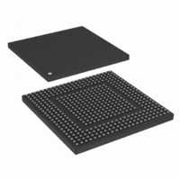
MPC8308-RDB Freescale Semiconductor, MPC8308-RDB Datasheet - Page 76

MPC8308-RDB
Manufacturer Part Number
MPC8308-RDB
Description
BOARD REF DESIGN MPC8308
Manufacturer
Freescale Semiconductor
Series
PowerQUICC II™ PROr
Type
MPUr
Datasheets
1.MPC8308VMAGD.pdf
(90 pages)
2.MPC8308VMAGD.pdf
(2 pages)
3.MPC8308-RDB.pdf
(36 pages)
4.MPC8308-RDB.pdf
(2 pages)
Specifications of MPC8308-RDB
Contents
Board, Cables, Documentation, Power Supply, Software
Ethernet Connection Type
Serial to Ethernet
Data Rate
10 Mbps, 100 Mbps, 1000 Mbps
Memory Type
DDR2, SDRAM
Interface Type
HSSI
Operating Voltage
1.5 V
Operating Current
5 uA
Maximum Power Dissipation
1000 mW
Operating Temperature Range
- 55 C to + 125 C
Product
Modules
For Use With/related Products
MPC8308
Lead Free Status / RoHS Status
Lead free / RoHS Compliant
Clocking
21 Clocking
Figure 53
1
2
The following external clock sources are utilized on the MPC8308:
All clock inputs can be supplied using an external canned oscillator, a clock generation chip, or some other
source that provides a standard CMOS square wave input.
76
Multiplication factor M = 1, 1.5, 2, 2.5, and 3. Value is decided by RCWLR[COREPLL].
Multiplication factor L = 2, 3, 4, 5 and 6. Value is decided by RCWLR[SPMF].
•
•
•
•
SYS_CLK_IN
24–66 MHz
SD_REF_CLK_B
SD_REF_CLK
125/100 MHz
System clock (SYS_CLK_IN)
Ethernet Clock (TSEC1_RX_CLK/TSEC1_TX_CLK/TSEC1_GTX_CLK125 for eTSEC)
SerDes PHY clock
eSHDC clock (SD_CLK)
For more information, see the SerDes chapter in the MPC8308 PowerQUICC II Pro Processor
Reference Manual.
SD_CLK
shows the internal distribution of clocks within the device.
MPC8308 PowerQUICC II Pro Processor Hardware Specification, Rev. 2
+
-
eSHDC
PLL
MPC8308
Figure 53. MPC8308 Clock Subsystem
PCVTR Mux
SerDes PHY
PCI Express
Converter
Protocol
x L
ref
System
PLL
2
fb
Gen
Clk
clk tree
x M
1
e300
PLL
e300 Core
ddr_clk
eTSEC1
lbc_clk
csb_clk
DDR
/n
Clock
Divider
LBC
Clock
Divider
/2
Freescale Semiconductor
MCK[0:2]
TSEC1_TX_CLK/
TSEC1_GTX_CLK125
TSEC1_RX_CLK
MCK[0:2]
Local
Bus
Memory
Device
DDR
Memory
Device


