C8051F540DK Silicon Laboratories Inc, C8051F540DK Datasheet - Page 13
C8051F540DK
Manufacturer Part Number
C8051F540DK
Description
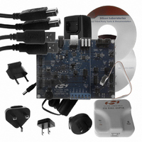
KIT DEVELOPMENT FOR C8051F540
Manufacturer
Silicon Laboratories Inc
Type
MCUr
Datasheet
1.C8051F540DK.pdf
(22 pages)
Specifications of C8051F540DK
Contents
Evaluation Board, Power Supply, USB Cables, Adapter and Documentation
Processor To Be Evaluated
C8051F54x
Processor Series
C8051F54x
Interface Type
USB
Operating Supply Voltage
5 V
Lead Free Status / RoHS Status
Lead free / RoHS Compliant
For Use With/related Products
C8051F54x
Lead Free Status / Rohs Status
Lead free / RoHS Compliant
Other names
336-1669


7.8. Port I/O Connectors (J1-J3 and J5-J7)
Each of the parallel ports of the C8051F540 (Side A) and C8051F542 (Side B) has its own 10-pin header
connector. Each connector provides a pin for the corresponding port pins 0–7, +5 V VIO, and digital ground. The
same pin-out is used for all of the port connectors.
Port 2 on the C8051F542 (Side B) MCU has only two pins and has a reduced header.
7.9. Voltage Reference (VREF) Connectors (J13 and J19)
The VREF connectors can be used to connect the VREF pin from the MCU (P0.0) to external 0.1 µF and 4.7 µF
decoupling capacitors. The C8051F540 (Side A) device is connected to the capacitors through the J13 header and
the C8051F542 (Side B) device connects to its own set of capacitors through J19.
7.10. Potentiometer (J17)
The C8051F540 (Side A) device has the option to connect port pin P1.2 to a 10K linear potentiometer. The
potentiometer is connected through the J17 header. The potentiometer can be used for testing the analog-to-digital
(ADC) converter of the MCU.
Table 7. Port I/O Connector Pin Description (J7)
Table 6. Port I/O Connector Pin Description
Pin #
Pin #
10
1
2
3
4
5
6
7
8
9
1
2
3
4
Rev. 0.1
Pin Description
Pin Description
GND (Ground)
GND (Ground)
+5V (VIO)
+5V (VIO)
Pn.0
Pn.1
Pn.2
Pn.3
Pn.4
Pn.5
Pn.6
Pn.7
Pn.0
Pn.1
C8051F540DK
13
Related parts for C8051F540DK
Image
Part Number
Description
Manufacturer
Datasheet
Request
R

Part Number:
Description:
SMD/C°/SINGLE-ENDED OUTPUT SILICON OSCILLATOR
Manufacturer:
Silicon Laboratories Inc
Part Number:
Description:
Manufacturer:
Silicon Laboratories Inc
Datasheet:
Part Number:
Description:
N/A N/A/SI4010 AES KEYFOB DEMO WITH LCD RX
Manufacturer:
Silicon Laboratories Inc
Datasheet:
Part Number:
Description:
N/A N/A/SI4010 SIMPLIFIED KEY FOB DEMO WITH LED RX
Manufacturer:
Silicon Laboratories Inc
Datasheet:
Part Number:
Description:
N/A/-40 TO 85 OC/EZLINK MODULE; F930/4432 HIGH BAND (REV E/B1)
Manufacturer:
Silicon Laboratories Inc
Part Number:
Description:
EZLink Module; F930/4432 Low Band (rev e/B1)
Manufacturer:
Silicon Laboratories Inc
Part Number:
Description:
I°/4460 10 DBM RADIO TEST CARD 434 MHZ
Manufacturer:
Silicon Laboratories Inc
Part Number:
Description:
I°/4461 14 DBM RADIO TEST CARD 868 MHZ
Manufacturer:
Silicon Laboratories Inc
Part Number:
Description:
I°/4463 20 DBM RFSWITCH RADIO TEST CARD 460 MHZ
Manufacturer:
Silicon Laboratories Inc
Part Number:
Description:
I°/4463 20 DBM RADIO TEST CARD 868 MHZ
Manufacturer:
Silicon Laboratories Inc
Part Number:
Description:
I°/4463 27 DBM RADIO TEST CARD 868 MHZ
Manufacturer:
Silicon Laboratories Inc
Part Number:
Description:
I°/4463 SKYWORKS 30 DBM RADIO TEST CARD 915 MHZ
Manufacturer:
Silicon Laboratories Inc
Part Number:
Description:
N/A N/A/-40 TO 85 OC/4463 RFMD 30 DBM RADIO TEST CARD 915 MHZ
Manufacturer:
Silicon Laboratories Inc
Part Number:
Description:
I°/4463 20 DBM RADIO TEST CARD 169 MHZ
Manufacturer:
Silicon Laboratories Inc