C8051F540DK Silicon Laboratories Inc, C8051F540DK Datasheet - Page 12
C8051F540DK
Manufacturer Part Number
C8051F540DK
Description
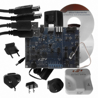
KIT DEVELOPMENT FOR C8051F540
Manufacturer
Silicon Laboratories Inc
Type
MCUr
Datasheet
1.C8051F540DK.pdf
(22 pages)
Specifications of C8051F540DK
Contents
Evaluation Board, Power Supply, USB Cables, Adapter and Documentation
Processor To Be Evaluated
C8051F54x
Processor Series
C8051F54x
Interface Type
USB
Operating Supply Voltage
5 V
Lead Free Status / RoHS Status
Lead free / RoHS Compliant
For Use With/related Products
C8051F54x
Lead Free Status / Rohs Status
Lead free / RoHS Compliant
Other names
336-1669


C8051F540DK
7.6. Serial Interface (P5, J14)
A USB-to-UART bridge device (U3) and USB connector (P5) are provided on the target board to facilitate serial
connections to UART0 of the C8051F540 (Side A). The Silicon Labs CP2102 USB-to-UART bridge provides data
connectivity between the C8051F540 and the PC via a USB port. The TX and RX signals of UART0 may be
connected to the CP2102 by installing shorting blocks on header J14. The shorting block positions for connecting
each of these signals to the CP2102 are listed in Table 3. To use this interface, the USB-to-UART device drivers
should be installed as described in Section 4.3. "CP210x USB to UART VCP Driver Installation‚" on page 3.
7.7. LIN Interface and Network (J12, J14, TB1)
Both MCUs on the target board are connected to LIN transceivers through headers. These headers assume that
the MCU’s crossbars are configured to put the LIN TX and RX pins on port pins P1.0 and P1.1 respectively. See
the C8051F54x data sheet for crossbar configuration. The C8051F540 (Side A) is connected to the T1 transceiver
through the J14 header and the C8051F542 (Side B) is connected to the T2 transceiver through the J12 header.
The two LIN transceivers are connected to each other and form a LIN network. Other external devices can be
connected to the LIN network through the TB1 interface. The TB1 interface also provides the option for connecting
an external power source so that all LIN transceivers can use the same source voltage. This source voltage can
also be used to power the target board. If an external voltage source is not provided, the LIN transceivers use the
12 V provided through the P1 power adapter connector. See Section 7.2. for more power option details. The
shorting block positions for connecting the MCUs to the LIN transceivers are listed in Table 4. The pin connections
for the external LIN devices are listed in Table 5.
12
Table 4. LIN Interface Headers (J12 and J14) Description
Table 5. TB1 External LIN Interface Header Description
Table 3. Serial Interface Header (J14) Description
Header Pins UART0 Pin Description
Header Pins
J14[3–4]
J14[1–2]
J14[5–6]
J14[7–8]
J12[3–3]
J12[1–2]
Pin #
1
2
3
LIN0 Pin Description
Rev. 0.1
UART_RX (P0.5_A)
UART_TX (P0.4_A)
Pin Description
LIN_TX (P1.0_A)
LIN_RX (P1.1_A)
LIN_TX (P1.0_B)
LIN_RX (P1.1_B)
LIN_OUT
+LIN_V
GND
Related parts for C8051F540DK
Image
Part Number
Description
Manufacturer
Datasheet
Request
R

Part Number:
Description:
SMD/C°/SINGLE-ENDED OUTPUT SILICON OSCILLATOR
Manufacturer:
Silicon Laboratories Inc
Part Number:
Description:
Manufacturer:
Silicon Laboratories Inc
Datasheet:
Part Number:
Description:
N/A N/A/SI4010 AES KEYFOB DEMO WITH LCD RX
Manufacturer:
Silicon Laboratories Inc
Datasheet:
Part Number:
Description:
N/A N/A/SI4010 SIMPLIFIED KEY FOB DEMO WITH LED RX
Manufacturer:
Silicon Laboratories Inc
Datasheet:
Part Number:
Description:
N/A/-40 TO 85 OC/EZLINK MODULE; F930/4432 HIGH BAND (REV E/B1)
Manufacturer:
Silicon Laboratories Inc
Part Number:
Description:
EZLink Module; F930/4432 Low Band (rev e/B1)
Manufacturer:
Silicon Laboratories Inc
Part Number:
Description:
I°/4460 10 DBM RADIO TEST CARD 434 MHZ
Manufacturer:
Silicon Laboratories Inc
Part Number:
Description:
I°/4461 14 DBM RADIO TEST CARD 868 MHZ
Manufacturer:
Silicon Laboratories Inc
Part Number:
Description:
I°/4463 20 DBM RFSWITCH RADIO TEST CARD 460 MHZ
Manufacturer:
Silicon Laboratories Inc
Part Number:
Description:
I°/4463 20 DBM RADIO TEST CARD 868 MHZ
Manufacturer:
Silicon Laboratories Inc
Part Number:
Description:
I°/4463 27 DBM RADIO TEST CARD 868 MHZ
Manufacturer:
Silicon Laboratories Inc
Part Number:
Description:
I°/4463 SKYWORKS 30 DBM RADIO TEST CARD 915 MHZ
Manufacturer:
Silicon Laboratories Inc
Part Number:
Description:
N/A N/A/-40 TO 85 OC/4463 RFMD 30 DBM RADIO TEST CARD 915 MHZ
Manufacturer:
Silicon Laboratories Inc
Part Number:
Description:
I°/4463 20 DBM RADIO TEST CARD 169 MHZ
Manufacturer:
Silicon Laboratories Inc