C8051F540DK Silicon Laboratories Inc, C8051F540DK Datasheet - Page 10
C8051F540DK
Manufacturer Part Number
C8051F540DK
Description
KIT DEVELOPMENT FOR C8051F540
Manufacturer
Silicon Laboratories Inc
Type
MCUr
Datasheet
1.C8051F540DK.pdf
(22 pages)
Specifications of C8051F540DK
Contents
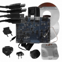
Evaluation Board, Power Supply, USB Cables, Adapter and Documentation
Processor To Be Evaluated
C8051F54x
Processor Series
C8051F54x
Interface Type
USB
Operating Supply Voltage
5 V
Lead Free Status / RoHS Status
Lead free / RoHS Compliant
For Use With/related Products
C8051F54x
Lead Free Status / Rohs Status
Lead free / RoHS Compliant
Other names
336-1669


C8051F540DK
7.2. Target Board Power Options and Current Measurement (J4, J8, J24, P1, TB1)
The MCUs on the C8051F540 Target Board are powered from a +5 V net. The +5 V net is connected to the
headers J8 (Side A) and J4 (Side B). Shorting blocks can be put on each header to connect the +5 V net to the
VREGIN and VIO pins on the two MCUs. With the shorting blocks removed, a source meter can be used across
the headers to measure the current consumption of the MCU.
The +5 V net on the target board has three possible sources:
7.2.1. Using the AC to DC Power Adapter as the Target Board Power Source (P1, P4)
The default configuration of the target board uses the ac to dc power adapter as the source. The 12 V from the
adapter is regulated to +5 V using an LDO regulator (U4). The output of the regulator is connected to the +5 V net
of the target board through the P4 header. A shorting block should be installed on pins P4[2–3] for this purpose.
The +5 V net powers the MCUs.
7.2.2. Using the USB Debug Adapter as the Target Board Power Source (P4)
The target board can use +5 V provided by the USB Debug Adapter. To enable this source, a shorting block should
be installed on pins P4[1-2]. With this shorting block, the output of the LDO regulator (U4) is disconnected from the
+5 V net of the target board, and the SER_PWR node is connected to +5 V.
Note: The USB Debug Adapter does not provide the necessary peak power for the CAN transceivers to operate.
One of the 12 V dc sources is recommended for CAN transceiver operation.
7.2.3. Using an External +12V LIN Source as the Target Board Power Source (P4, TB1)
The two 12 V power sources (LIN and ac to dc power adapter) are ORed together using reverse-biased diodes (Z1
and Z2) and connected to the input of the LDO regulator (U6). The output of the regulator is connected to the +5 V
net of the target board through the P4 header. A shorting block should be installed on pins P4[2-3] for this purpose.
The +5 V net powers the MCUs directly.
7.3. System Clock Sources (J9, J10)
7.3.1. Internal Oscillators
The C8051F540 and C8051F542 devices installed on the target board feature a factory-calibrated, programmable
high-frequency internal oscillator (24 MHz base frequency, ±0.5%), which is enabled as the system clock source on
reset. After reset, the internal oscillator operates at a frequency of 187.5 kHz by default but may be configured by
software to operate at other frequencies. The on-chip crystal is accurate for LIN master communications and in
many applications an external oscillator is not required. However, if you wish to operate the C8051F540 device
(Side A) at a frequency not available with the internal oscillator, an external crystal may be used. Refer to the
C8051F54x data sheet for more information on configuring the system clock source.
7.3.2. External Oscillator Options
The target board is designed to facilitate the installation of an external crystal. Remove shorting blocks at headers
J9 and J10 and install the crystal at the pads marked Y1. Install a 10 M resistor at R2 and install capacitors at C7
and C8 using values appropriate for the crystal you select. If you wish to operate the external oscillator in capacitor
or RC mode, options to install a capacitor or an RC network are also available on the target board. R2, R3, C7, and
C8 are located on the back side of the board, near the Side A MCU. Populate C7 for capacitor mode, and populate
R3 and C7 for RC mode. Refer to the C8051F54x data sheet for more information on the use of external
oscillators.
10
1. 12 V dc power using the ac to dc power adapter (P1)
2. 5 V dc USB VBUS power from PC via the USB Debug Adapter (DEBUG_A)
3. 12 V dc power from the LIN external header (TB1)
Rev. 0.1
Related parts for C8051F540DK
Image
Part Number
Description
Manufacturer
Datasheet
Request
R

Part Number:
Description:
SMD/C°/SINGLE-ENDED OUTPUT SILICON OSCILLATOR
Manufacturer:
Silicon Laboratories Inc
Part Number:
Description:
Manufacturer:
Silicon Laboratories Inc
Datasheet:
Part Number:
Description:
N/A N/A/SI4010 AES KEYFOB DEMO WITH LCD RX
Manufacturer:
Silicon Laboratories Inc
Datasheet:
Part Number:
Description:
N/A N/A/SI4010 SIMPLIFIED KEY FOB DEMO WITH LED RX
Manufacturer:
Silicon Laboratories Inc
Datasheet:
Part Number:
Description:
N/A/-40 TO 85 OC/EZLINK MODULE; F930/4432 HIGH BAND (REV E/B1)
Manufacturer:
Silicon Laboratories Inc
Part Number:
Description:
EZLink Module; F930/4432 Low Band (rev e/B1)
Manufacturer:
Silicon Laboratories Inc
Part Number:
Description:
I°/4460 10 DBM RADIO TEST CARD 434 MHZ
Manufacturer:
Silicon Laboratories Inc
Part Number:
Description:
I°/4461 14 DBM RADIO TEST CARD 868 MHZ
Manufacturer:
Silicon Laboratories Inc
Part Number:
Description:
I°/4463 20 DBM RFSWITCH RADIO TEST CARD 460 MHZ
Manufacturer:
Silicon Laboratories Inc
Part Number:
Description:
I°/4463 20 DBM RADIO TEST CARD 868 MHZ
Manufacturer:
Silicon Laboratories Inc
Part Number:
Description:
I°/4463 27 DBM RADIO TEST CARD 868 MHZ
Manufacturer:
Silicon Laboratories Inc
Part Number:
Description:
I°/4463 SKYWORKS 30 DBM RADIO TEST CARD 915 MHZ
Manufacturer:
Silicon Laboratories Inc
Part Number:
Description:
N/A N/A/-40 TO 85 OC/4463 RFMD 30 DBM RADIO TEST CARD 915 MHZ
Manufacturer:
Silicon Laboratories Inc
Part Number:
Description:
I°/4463 20 DBM RADIO TEST CARD 169 MHZ
Manufacturer:
Silicon Laboratories Inc