C8051F206DK Silicon Laboratories Inc, C8051F206DK Datasheet - Page 72
C8051F206DK
Manufacturer Part Number
C8051F206DK
Description
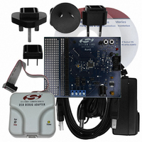
DEV KIT FOR C8051F206
Manufacturer
Silicon Laboratories Inc
Type
MCUr
Specifications of C8051F206DK
Contents
Evaluation Board, Power Supply, USB Cables, Adapter and Documentation
Processor To Be Evaluated
C8051F206
Interface Type
USB
Lead Free Status / RoHS Status
Contains lead / RoHS non-compliant
For Use With/related Products
Silicon Laboratories C8051F206
Lead Free Status / Rohs Status
Lead free / RoHS Compliant
Other names
336-1237


C8051F2xx
72
Bit7:
Bit6:
Bit5:
Bits4–3: RS1–RS0: Register Bank Select.
Bit2:
Bit1:
Bit0:
R/W
CY
Bit7
RS1
CY: Carry Flag.
This bit is set when the last arithmetic operation results in a carry (addition) or a borrow
(subtraction). It is cleared to 0 by all other arithmetic operations.
AC: Auxiliary Carry Flag.
This bit is set when the last arithmetic operation results in a carry into (addition) or a borrow
from (subtraction) the high order nibble. It is cleared to 0 by all other arithmetic operations.
F0: User Flag 0.
This is a bit-addressable, general-purpose flag for use under software control.
These bits select which register bank is used during register accesses.
Note: Any instruction which changes the RS1–RS0 bits must not be immediately followed by
the “MOV Rn, A” instruction.
OV: Overflow Flag.
This bit is set to 1 under the following circumstances:
•An ADD, ADDC, or SUBB instruction causes a sign-change overflow.
•A MUL instruction results in an overflow (result is greater than 255).
•A DIV instruction causes a divide-by-zero condition.
The OV bit is cleared to 0 by the ADD, ADDC, SUBB, MUL, and DIV instructions in all other
cases.
F1: User Flag 1.
This is a bit-addressable, general purpose flag for use under software control.
PARITY: Parity Flag.
This bit is set to 1 if the sum of the eight bits in the accumulator is odd and cleared if the sum
is even.
0
0
1
1
R/W
AC
Bit6
RS0
0
1
0
1
SFR Definition 9.4. PSW: Program Status Word
R/W
Bit5
F0
Register Bank
0
1
2
3
RS1
R/W
Bit4
0x08–0x0F
0x18–0x1F
0x00–0x07
0x10–0x17
Rev. 1.6
Address
RS0
R/W
Bit3
R/W
OV
Bit2
R/W
Bit1
F1
addressable)
PARITY
Bit0
(bit
R
SFR Address:
Reset Value
00000000
0xD0
Related parts for C8051F206DK
Image
Part Number
Description
Manufacturer
Datasheet
Request
R

Part Number:
Description:
SMD/C°/SINGLE-ENDED OUTPUT SILICON OSCILLATOR
Manufacturer:
Silicon Laboratories Inc
Part Number:
Description:
Manufacturer:
Silicon Laboratories Inc
Datasheet:
Part Number:
Description:
N/A N/A/SI4010 AES KEYFOB DEMO WITH LCD RX
Manufacturer:
Silicon Laboratories Inc
Datasheet:
Part Number:
Description:
N/A N/A/SI4010 SIMPLIFIED KEY FOB DEMO WITH LED RX
Manufacturer:
Silicon Laboratories Inc
Datasheet:
Part Number:
Description:
N/A/-40 TO 85 OC/EZLINK MODULE; F930/4432 HIGH BAND (REV E/B1)
Manufacturer:
Silicon Laboratories Inc
Part Number:
Description:
EZLink Module; F930/4432 Low Band (rev e/B1)
Manufacturer:
Silicon Laboratories Inc
Part Number:
Description:
I°/4460 10 DBM RADIO TEST CARD 434 MHZ
Manufacturer:
Silicon Laboratories Inc
Part Number:
Description:
I°/4461 14 DBM RADIO TEST CARD 868 MHZ
Manufacturer:
Silicon Laboratories Inc
Part Number:
Description:
I°/4463 20 DBM RFSWITCH RADIO TEST CARD 460 MHZ
Manufacturer:
Silicon Laboratories Inc
Part Number:
Description:
I°/4463 20 DBM RADIO TEST CARD 868 MHZ
Manufacturer:
Silicon Laboratories Inc
Part Number:
Description:
I°/4463 27 DBM RADIO TEST CARD 868 MHZ
Manufacturer:
Silicon Laboratories Inc
Part Number:
Description:
I°/4463 SKYWORKS 30 DBM RADIO TEST CARD 915 MHZ
Manufacturer:
Silicon Laboratories Inc
Part Number:
Description:
N/A N/A/-40 TO 85 OC/4463 RFMD 30 DBM RADIO TEST CARD 915 MHZ
Manufacturer:
Silicon Laboratories Inc
Part Number:
Description:
I°/4463 20 DBM RADIO TEST CARD 169 MHZ
Manufacturer:
Silicon Laboratories Inc