Z8F083A0128ZCOG Zilog, Z8F083A0128ZCOG Datasheet - Page 5
Z8F083A0128ZCOG
Manufacturer Part Number
Z8F083A0128ZCOG
Description
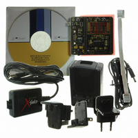
KIT DEVELOPMENT F083A
Manufacturer
Zilog
Series
Z8 Encore! XP®r
Type
MCUr
Specifications of Z8F083A0128ZCOG
Contents
Hardware, Software and Documentation
For Use With/related Products
Z8F083A
For Use With
269-4661 - KIT ACC ETHERNET SMART CABLE
Lead Free Status / RoHS Status
Lead free / RoHS Compliant
Other names
269-4672
Available stocks
Company
Part Number
Manufacturer
Quantity
Price
Company:

Part Number:
Z8F083A0128ZCOG
Manufacturer:
Zilog
Quantity:
1


PRS001003-1207
Flash Bypass Mode Register Structure
Table 2. User Mode Truth Table (Continued)
Table 3. IFREN Truth Table
To facilitate using Flash controller bypass mode for all package sizes, all the signals are
registered internally, allowing all data access to occur through a single 8-bit GPIO port
(Port A). Among the three other GPIO port pins (PortB1, PortB0, and PortC0), select one
of the input data registers or the data output register as shown in
In Flash test mode, PortA[7:0] becomes an input/output data port, and PortB[1], PortB[0],
and PortC[0] form a three input register address select as shown in
When TESTMODE pad is asserted, which is equal to 0 then:
•
•
•
•
Sector
Erase
Mass
Erase
Mode
Read
Program
Sector Erase
Mass Erase
*X stands for don’t care, and it is necessary to bias at either "H" or "L", L stands for logic Low, H
stands for logic High, and Z stands for High impedance.
PadTM[0] is shared with PortB7.
PadTM[1] is shared with PortC4.
PadTM[2] is shared with PortC5.
PadTM[3] is shared with PortC6.
H
H
H
H
L
L
IFREN=1
Read information block
Program information block
Erase information block
Erase both block
L
L
H
L
L
H
X
X
IFREN=0
Read main memory block
Program main memory block
Erase selected sector
Erase main memory block
Z
Z
Z8 Encore!
Active Active
X
Table
Table
4.
®
Active
4.
F083x Series
Page 5 of 25
Active
Active
Related parts for Z8F083A0128ZCOG
Image
Part Number
Description
Manufacturer
Datasheet
Request
R

Part Number:
Description:
Communication Controllers, ZILOG INTELLIGENT PERIPHERAL CONTROLLER (ZIP)
Manufacturer:
Zilog, Inc.
Datasheet:

Part Number:
Description:
KIT DEV FOR Z8 ENCORE 16K TO 64K
Manufacturer:
Zilog
Datasheet:

Part Number:
Description:
KIT DEV Z8 ENCORE XP 28-PIN
Manufacturer:
Zilog
Datasheet:

Part Number:
Description:
DEV KIT FOR Z8 ENCORE 8K/4K
Manufacturer:
Zilog
Datasheet:

Part Number:
Description:
KIT DEV Z8 ENCORE XP 28-PIN
Manufacturer:
Zilog
Datasheet:

Part Number:
Description:
DEV KIT FOR Z8 ENCORE 4K TO 8K
Manufacturer:
Zilog
Datasheet:
Part Number:
Description:
CMOS Z8 microcontroller. ROM 16 Kbytes, RAM 256 bytes, speed 16 MHz, 32 lines I/O, 3.0V to 5.5V
Manufacturer:
Zilog, Inc.
Datasheet:
Part Number:
Description:
Low-cost microcontroller. 512 bytes ROM, 61 bytes RAM, 8 MHz
Manufacturer:
Zilog, Inc.
Datasheet:
Part Number:
Description:
Z8 4K OTP Microcontroller
Manufacturer:
Zilog, Inc.
Datasheet:
Part Number:
Description:
CMOS SUPER8 ROMLESS MCU
Manufacturer:
Zilog, Inc.
Datasheet:
Part Number:
Description:
SL1866 CMOSZ8 OTP Microcontroller
Manufacturer:
Zilog, Inc.
Datasheet:
Part Number:
Description:
SL1866 CMOSZ8 OTP Microcontroller
Manufacturer:
Zilog, Inc.
Datasheet:
Part Number:
Description:
OTP (KB) = 1, RAM = 125, Speed = 12, I/O = 14, 8-bit Timers = 2, Comm Interfaces Other Features = Por, LV Protect, Voltage = 4.5-5.5V
Manufacturer:
Zilog, Inc.
Datasheet:
Part Number:
Description:
Manufacturer:
Zilog, Inc.
Datasheet: