Z8F083A0128ZCOG Zilog, Z8F083A0128ZCOG Datasheet - Page 3
Z8F083A0128ZCOG
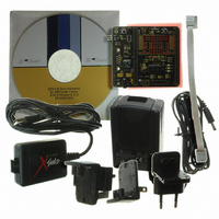
Manufacturer Part Number
Z8F083A0128ZCOG
Description
KIT DEVELOPMENT F083A
Manufacturer
Zilog
Series
Z8 Encore! XP®r
Type
MCUr
Specifications of Z8F083A0128ZCOG
Contents
Hardware, Software and Documentation
For Use With/related Products
Z8F083A
For Use With
269-4661 - KIT ACC ETHERNET SMART CABLE
Lead Free Status / RoHS Status
Lead free / RoHS Compliant
Other names
269-4672
Available stocks
Company
Part Number
Manufacturer
Quantity
Price
Company:

Part Number:
Z8F083A0128ZCOG
Manufacturer:
Zilog
Quantity:
1


Bypassing the Flash Controller
PRS001003-1207
Flash Test Mode Entry Prevention
Entering Flash Test Mode
Flash Memory Control Signals
If, IWP[3:0] (bits 7:4 at Flash Information Area address FE05H) is set to 0110b and FWP
(bit 2 of Program Memory address 0000H) is set to 0, then Flash test mode cannot be
entered. Program Memory is erased through the OCD, disabling the Flash read protect and
then allowing entry into Flash test mode.
Flash test mode can be entered in two ways.
1. One way is to drive the TESTMODE pad Low. The TESTMODE pad is accessible
2. Flash test mode can also be entered by setting bit 2 in the OCDs test mode register
Flash controller bypass mode is enabled by writing three bytes to the OCD via the DBG
interface.
1. 80H—Initiates auto-baud calculation of the DBG interface data and clock rate.
2. F0H—OCD write testmode register command.
3. 04H—Data to be written to the testmode register. This enables Flash controller bypass
Depending on the size (number of bytes) available in the Flash memory, the Flash memory
makes use of 38 signals.
•
•
•
•
before the part is packaged.
to 1.
mode.
14 signals for the address lines.
8 signals for data input.
8 signals for data output.
8 user mode control signals.
Z8 Encore!
®
F083x Series
Page 3 of 25
Related parts for Z8F083A0128ZCOG
Image
Part Number
Description
Manufacturer
Datasheet
Request
R

Part Number:
Description:
Communication Controllers, ZILOG INTELLIGENT PERIPHERAL CONTROLLER (ZIP)
Manufacturer:
Zilog, Inc.
Datasheet:

Part Number:
Description:
KIT DEV FOR Z8 ENCORE 16K TO 64K
Manufacturer:
Zilog
Datasheet:

Part Number:
Description:
KIT DEV Z8 ENCORE XP 28-PIN
Manufacturer:
Zilog
Datasheet:

Part Number:
Description:
DEV KIT FOR Z8 ENCORE 8K/4K
Manufacturer:
Zilog
Datasheet:

Part Number:
Description:
KIT DEV Z8 ENCORE XP 28-PIN
Manufacturer:
Zilog
Datasheet:

Part Number:
Description:
DEV KIT FOR Z8 ENCORE 4K TO 8K
Manufacturer:
Zilog
Datasheet:
Part Number:
Description:
CMOS Z8 microcontroller. ROM 16 Kbytes, RAM 256 bytes, speed 16 MHz, 32 lines I/O, 3.0V to 5.5V
Manufacturer:
Zilog, Inc.
Datasheet:
Part Number:
Description:
Low-cost microcontroller. 512 bytes ROM, 61 bytes RAM, 8 MHz
Manufacturer:
Zilog, Inc.
Datasheet:
Part Number:
Description:
Z8 4K OTP Microcontroller
Manufacturer:
Zilog, Inc.
Datasheet:
Part Number:
Description:
CMOS SUPER8 ROMLESS MCU
Manufacturer:
Zilog, Inc.
Datasheet:
Part Number:
Description:
SL1866 CMOSZ8 OTP Microcontroller
Manufacturer:
Zilog, Inc.
Datasheet:
Part Number:
Description:
SL1866 CMOSZ8 OTP Microcontroller
Manufacturer:
Zilog, Inc.
Datasheet:
Part Number:
Description:
OTP (KB) = 1, RAM = 125, Speed = 12, I/O = 14, 8-bit Timers = 2, Comm Interfaces Other Features = Por, LV Protect, Voltage = 4.5-5.5V
Manufacturer:
Zilog, Inc.
Datasheet:
Part Number:
Description:
Manufacturer:
Zilog, Inc.
Datasheet: