DK-DEV-4SGX230N Altera, DK-DEV-4SGX230N Datasheet - Page 68
DK-DEV-4SGX230N
Manufacturer Part Number
DK-DEV-4SGX230N
Description
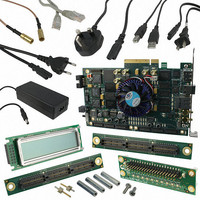
KIT DEVELOPMENT STRATIX IV
Manufacturer
Altera
Series
Stratix® IVr
Type
FPGAr
Datasheets
1.EP4SGX110DF29C3N.pdf
(80 pages)
2.EP4SGX110DF29C3N.pdf
(1154 pages)
3.DK-DEV-4SGX230N.pdf
(2 pages)
4.DK-DEV-4SGX530N.pdf
(57 pages)
Specifications of DK-DEV-4SGX230N
Contents
Development Board, Universal Power Supply, Cables and Software
Silicon Manufacturer
Altera
Core Architecture
FPGA
Core Sub-architecture
Stratix
Silicon Core Number
EP4S
Silicon Family Name
Stratix IV GX
Rohs Compliant
Yes
For Use With/related Products
EP4SGX230K
Lead Free Status / RoHS Status
Lead free / RoHS Compliant
Other names
544-2594
Available stocks
Company
Part Number
Manufacturer
Quantity
Price
Company:

Part Number:
DK-DEV-4SGX230N
Manufacturer:
Altera
Quantity:
135


1–60
Table 1–48. Memory Output Clock Jitter Specification for Stratix IV Devices
Table 1–49. OCT Calibration Block Specifications for Stratix IV Devices
Stratix IV Device Handbook Volume 4: Device Datasheet and Addendum
Clock period jitter
Cycle-to-cycle period jitter
Duty cycle jitter
Clock period jitter
Cycle-to-cycle period jitter
Duty cycle jitter
Notes to
(1) The memory output clock jitter measurements are for 200 consecutive clock cycles, as specified in the JEDEC DDR2/DDR3 SDRAM standard.
(2) The clock jitter specification applies to memory output clock pins generated using differential signal-splitter and DDIO circuits clocked by a PLL
(3) The memory output clock jitter stated in
OCTUSRCLK
T
T
T
OCTCAL
OCTSHIFT
RS_RT
output routed on a regional or global clock network as specified. Altera recommends using regional clock networks whenever possible.
Symbol
Table
Parameter
1–48:
1
1
Number of OCTUSRCLK clock cycles required for OCT R
calibration
Number of OCTUSRCLK clock cycles required for OCT code
to shift out
Time required between the dyn_term_ctrl and oe signal
transitions in a bidirectional I/O buffer to dynamically switch
between OCT R
Clock required by OCT calibration blocks
For the Stratix IV GT –1 and –2 speed grade specifications, refer to the –2/–2× speed
grade column. For the Stratix IV GT –3 speed grade specification, refer to the –3 speed
grade column.
Table 1–48
For the Stratix IV GT –1 and –2 speed grade specifications, refer to the –2/–2× speed
grade column. For the Stratix IV GT –3 speed grade specification, refer to the –3 speed
grade column.
OCT Calibration Block Specifications
Table 1–49
Regional
Regional
Regional
Network
Global
Global
Global
Clock
S
and R
lists the memory output clock jitter specifications for Stratix IV devices.
lists the OCT calibration block specifications for Stratix IV devices.
Table 1–48
T
Description
Symbol
t
t
t
t
t
JIT(duty)
t
JIT(duty)
JIT(per)
JIT(per)
JIT(cc)
JIT(cc)
is applicable when an input jitter of 30 ps is applied.
-100
-150
Min
-50
-50
-75
-75
Speed Grade
–2/–2X
Chapter 1: DC and Switching Characteristics for Stratix IV Devices
Max
100
150
50
50
75
75
S
/R
-82.5
-82.5
-110
-165
Min
-55
-90
T
Speed Grade
(Note
–3
Min
—
—
—
—
1), (2),
82.5
82.5
Max
110
165
55
90
1000
(3)
Typ
2.5
—
28
-82.5
-82.5
-110
-165
April 2011 Altera Corporation
Min
-55
-90
Speed Grade
Switching Characteristics
–4
Max
20
—
—
—
Max
82.5
82.5
110
165
55
90
Cycles
Cycles
MHz
Unit
ns
Unit
ps
ps
ps
ps
ps
ps
Related parts for DK-DEV-4SGX230N
Image
Part Number
Description
Manufacturer
Datasheet
Request
R

Part Number:
Description:
KIT DEV ARRIA II GX FPGA 2AGX125
Manufacturer:
Altera
Datasheet:

Part Number:
Description:
KIT DEV CYCLONE III LS EP3CLS200
Manufacturer:
Altera
Datasheet:

Part Number:
Description:
KIT DEV STRATIX IV FPGA 4SE530
Manufacturer:
Altera
Datasheet:

Part Number:
Description:
KIT DEV FPGA 2AGX260 W/6.375G TX
Manufacturer:
Altera
Datasheet:

Part Number:
Description:
KIT DEV MAX V 5M570Z
Manufacturer:
Altera
Datasheet:

Part Number:
Description:
KIT DEV STRATIX V FPGA 5SGXEA7
Manufacturer:
Altera
Datasheet:

Part Number:
Description:
KIT DEVELOPMENT STRATIX III
Manufacturer:
Altera
Datasheet:

Part Number:
Description:
KIT DEV ARRIA GX 1AGX60N
Manufacturer:
Altera
Datasheet:
Part Number:
Description:
KIT STARTER CYCLONE IV GX
Manufacturer:
Altera
Datasheet:
Part Number:
Description:
KIT DEVELOPMENT STRATIX IV
Manufacturer:
Altera
Datasheet:

Part Number:
Description:
CPLD, EP610 Family, ECMOS Process, 300 Gates, 16 Macro Cells, 16 Reg., 16 User I/Os, 5V Supply, 35 Speed Grade, 24DIP
Manufacturer:
Altera Corporation
Datasheet:
Part Number:
Description:
CPLD, EP610 Family, ECMOS Process, 300 Gates, 16 Macro Cells, 16 Reg., 16 User I/Os, 5V Supply, 15 Speed Grade, 24DIP
Manufacturer:
Altera Corporation
Datasheet: