DK-DEV-4SGX230N Altera, DK-DEV-4SGX230N Datasheet - Page 58
DK-DEV-4SGX230N
Manufacturer Part Number
DK-DEV-4SGX230N
Description
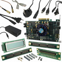
KIT DEVELOPMENT STRATIX IV
Manufacturer
Altera
Series
Stratix® IVr
Type
FPGAr
Datasheets
1.EP4SGX110DF29C3N.pdf
(80 pages)
2.EP4SGX110DF29C3N.pdf
(1154 pages)
3.DK-DEV-4SGX230N.pdf
(2 pages)
4.DK-DEV-4SGX530N.pdf
(57 pages)
Specifications of DK-DEV-4SGX230N
Contents
Development Board, Universal Power Supply, Cables and Software
Silicon Manufacturer
Altera
Core Architecture
FPGA
Core Sub-architecture
Stratix
Silicon Core Number
EP4S
Silicon Family Name
Stratix IV GX
Rohs Compliant
Yes
For Use With/related Products
EP4SGX230K
Lead Free Status / RoHS Status
Lead free / RoHS Compliant
Other names
544-2594
Available stocks
Company
Part Number
Manufacturer
Quantity
Price
Company:

Part Number:
DK-DEV-4SGX230N
Manufacturer:
Altera
Quantity:
135


1–50
Stratix IV Device Handbook Volume 4: Device Datasheet and Addendum
Configuration and JTAG Specifications
Table 1–37
Table 1–37. Configuration Mode Specifications for Stratix IV Devices—Preliminary
Table 1–38
Table 1–38. JTAG Timing Parameters and Values for Stratix IV Devices—Preliminary
Temperature Sensing Diode Specifications
Table 1–39
Table 1–39. External Temperature Sensing Diode Specifications—Preliminary
Passive serial
Fast passive parallel
Fast active serial
Remote update only in fast AS mode
Note to
(1) This denotes the maximum frequency supported in the FPP configuration scheme. The frequency supported for
t
t
t
t
t
t
t
t
t
Note to
(1) A 1 ns adder is required for each V
I
V
Series resistance
Diode ideality factor
JCP
JCH
JCL
JPSU (TDI)
JPSU (TMS)
JPH
JPCO
JPZX
JPXZ
bias
bias,
Symbol
, diode source current
each device may vary depending on device density. For more information, refer to the
Security, and Remote System Upgrades in Stratix IV Devices
I/O bank = 2.5 V, or 13 ns if it equals 1.8 V.
voltage across diode
Table
Table
lists the Stratix IV configuration mode specifications.
lists the JTAG timing parameters and values for Stratix IV devices.
lists the specifications for the Stratix IV temperature sensing diode.
1–37:
1–38:
Programming Mode
Description
TCK clock period
TCK clock high time
TCK clock low time
TDI JTAG port setup time
TMS JTAG port setup time
JTAG port hold time
JTAG port clock to output
JTAG port high impedance to valid output
JTAG port valid output to high impedance
(1)
CCIO
Description
voltage step down from 3.0 V. For example, t
Chapter 1: DC and Switching Characteristics for Stratix IV Devices
Min
0.3
—
—
8
Min
4.3
—
—
17
chapter.
DCLK F
Typ
—
—
—
—
Typ
5.3
—
—
26
Min
30
14
14
—
—
—
1
3
5
MAX
JPCO
April 2011 Altera Corporation
Configuration, Design
= 12 ns if V
11
14
14
1.030
Switching Characteristics
Max
Max
500
125
125
Max
0.9
< 5
40
10
—
—
—
—
—
—
(1)
(1)
(1)
CCIO
of the TDO
MHz
MHz
MHz
MHz
Unit
Unit
Unit
μA
—
ns
ns
ns
ns
ns
ns
ns
ns
ns
Ω
V
Related parts for DK-DEV-4SGX230N
Image
Part Number
Description
Manufacturer
Datasheet
Request
R

Part Number:
Description:
KIT DEV ARRIA II GX FPGA 2AGX125
Manufacturer:
Altera
Datasheet:

Part Number:
Description:
KIT DEV CYCLONE III LS EP3CLS200
Manufacturer:
Altera
Datasheet:

Part Number:
Description:
KIT DEV STRATIX IV FPGA 4SE530
Manufacturer:
Altera
Datasheet:

Part Number:
Description:
KIT DEV FPGA 2AGX260 W/6.375G TX
Manufacturer:
Altera
Datasheet:

Part Number:
Description:
KIT DEV MAX V 5M570Z
Manufacturer:
Altera
Datasheet:

Part Number:
Description:
KIT DEV STRATIX V FPGA 5SGXEA7
Manufacturer:
Altera
Datasheet:

Part Number:
Description:
KIT DEVELOPMENT STRATIX III
Manufacturer:
Altera
Datasheet:

Part Number:
Description:
KIT DEV ARRIA GX 1AGX60N
Manufacturer:
Altera
Datasheet:
Part Number:
Description:
KIT STARTER CYCLONE IV GX
Manufacturer:
Altera
Datasheet:
Part Number:
Description:
KIT DEVELOPMENT STRATIX IV
Manufacturer:
Altera
Datasheet:

Part Number:
Description:
CPLD, EP610 Family, ECMOS Process, 300 Gates, 16 Macro Cells, 16 Reg., 16 User I/Os, 5V Supply, 35 Speed Grade, 24DIP
Manufacturer:
Altera Corporation
Datasheet:
Part Number:
Description:
CPLD, EP610 Family, ECMOS Process, 300 Gates, 16 Macro Cells, 16 Reg., 16 User I/Os, 5V Supply, 15 Speed Grade, 24DIP
Manufacturer:
Altera Corporation
Datasheet: