MPC8313E-RDBB Freescale Semiconductor, MPC8313E-RDBB Datasheet - Page 27
MPC8313E-RDBB
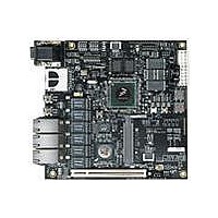
Manufacturer Part Number
MPC8313E-RDBB
Description
BOARD CPU 8313E VER 2.1
Manufacturer
Freescale Semiconductor
Series
PowerQUICC II™ PROr
Type
MPUr
Datasheets
1.MPC8313CZQAFFB.pdf
(100 pages)
2.MPC8313E-RDBB.pdf
(52 pages)
3.MPC8313E-RDBB.pdf
(2 pages)
Specifications of MPC8313E-RDBB
Contents
Board
Processor To Be Evaluated
MPC8xxx
Data Bus Width
32 bit
Interface Type
Ethernet, USB, JTAG, SPI, UART
Dimensions
170 mm x 170 mm
Operating Supply Voltage
3.3 V
For Use With/related Products
MPC8313E
Lead Free Status / RoHS Status
Lead free / RoHS Compliant


Figure 14
Freescale Semiconductor
At recommended operating conditions with LV
Duty cycle for 10BASE-T and 100BASE-TX
Rise time (20%–80%)
Fall time (20%–80%)
GTX_CLK125 reference clock period
GTX_CLK125 reference clock duty cycle
Notes:
1. Note that, in general, the clock reference symbol representation for this section is based on the symbols RGT to represent
2. This implies that PC board design requires clocks to be routed such that an additional trace delay of greater than 1.5 ns is
3. For 10 and 100 Mbps, t
4. Duty cycle may be stretched/shrunk during speed changes or while transitioning to a received packet's clock domains as long
5. Duty cycle reference is LV
6. This symbol is used to represent the external GTX_CLK125 and does not follow the original symbol naming convention.
RGMII and RTBI timing. For example, the subscript of t
notation for rise (R) and fall (F) times follows the clock symbol that is being represented. For symbols representing skews,
the subscript is skew (SK) followed by the clock that is being skewed (RGT).
added to the associated clock signal.
as the minimum duty cycle is not violated and stretching occurs for no more than three t
between.
(At Transmitter)
shows the RGMII and RTBI AC timing and multiplexing diagrams.
RXD[8:5][3:0]
RXD[7:4][3:0]
TXD[8:5][3:0]
TXD[7:4][3:0]
GTX_CLK
(At PHY)
(At PHY)
RX_CTL
RX_CLK
TX_CLK
TX_CTL
Parameter/Condition
MPC8313E PowerQUICC
Figure 14. RGMII and RTBI AC Timing and Multiplexing Diagrams
Table 30. RGMII and RTBI AC Timing Specifications (continued)
RGT
DDA
scales to 400 ns ± 40 ns and 40 ns ± 4 ns, respectively.
/2 or LV
DDB
DDA
RXD[3:0]
TXD[3:0]
RXD[4]
TXD[4]
TXEN
RXDV
/LV
/2.
3, 5
DDB
™
of 2.5 V ± 5%.
II Pro Processor Hardware Specifications, Rev. 3
RXD[8:5]
RXD[7:4]
TXD[8:5]
TXD[7:4]
RXERR
TXERR
RXD[9]
TXD[9]
RGT
represents the RTBI (T) receive (RX) clock. Note also that the
t
t
G125H
RGTH
Symbol
t
t
t
RGTR
G12
RGTF
/t
/t
RGT
G125
6
1
t
t
SKRGT
SKRGT
t
RGTH
Ethernet: Three-Speed Ethernet, MII Management
Min
40
47
—
—
—
RGT
t
of the lowest speed transitioned
RGT
Typ
8.0
50
—
—
—
t
t
SKRGT
SKRGT
Max
0.75
0.75
60
53
—
Unit
ns
ns
ns
%
%
27
Related parts for MPC8313E-RDBB
Image
Part Number
Description
Manufacturer
Datasheet
Request
R

Part Number:
Description:
Mpc8313e Powerquicc Ii Pro Processor
Manufacturer:
Freescale Semiconductor, Inc
Datasheet:

Part Number:
Description:
BOARD PROCESSOR
Manufacturer:
Freescale Semiconductor
Datasheet:

Part Number:
Description:
BOARD CPU 8313E VER 2.2
Manufacturer:
Freescale Semiconductor
Datasheet:
Part Number:
Description:
Microprocessors - MPU 8313 REV2.2 PB ENC EXT
Manufacturer:
Freescale Semiconductor
Datasheet:
Part Number:
Description:
Microprocessors - MPU 8313 REV2.2 PB W/ENC
Manufacturer:
Freescale Semiconductor
Datasheet:
Part Number:
Description:
Microprocessors - MPU 8313 REV2.2 PB NO EN EXT
Manufacturer:
Freescale Semiconductor
Datasheet:
Part Number:
Description:
Microprocessors - MPU 8313 REV2.2 PB NO ENC
Manufacturer:
Freescale Semiconductor
Datasheet:
Part Number:
Description:
Manufacturer:
Freescale Semiconductor, Inc
Datasheet:
Part Number:
Description:
Manufacturer:
Freescale Semiconductor, Inc
Datasheet:
Part Number:
Description:
Manufacturer:
Freescale Semiconductor, Inc
Datasheet:
Part Number:
Description:
Manufacturer:
Freescale Semiconductor, Inc
Datasheet:
Part Number:
Description:
Manufacturer:
Freescale Semiconductor, Inc
Datasheet:
Part Number:
Description:
Manufacturer:
Freescale Semiconductor, Inc
Datasheet:
Part Number:
Description:
Manufacturer:
Freescale Semiconductor, Inc
Datasheet:
Part Number:
Description:
Manufacturer:
Freescale Semiconductor, Inc
Datasheet: