M68EVB908QL4 Freescale Semiconductor, M68EVB908QL4 Datasheet - Page 8
M68EVB908QL4
Manufacturer Part Number
M68EVB908QL4
Description
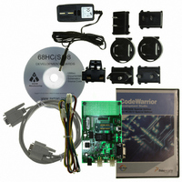
BOARD EVALUATION FOR 908QL4 MCU
Manufacturer
Freescale Semiconductor
Type
MCUr
Datasheet
1.M68EVB908QL4.pdf
(13 pages)
Specifications of M68EVB908QL4
Contents
Module and Misc Hardware
For Use With/related Products
MC68HC908QL4 Family
Lead Free Status / RoHS Status
Contains lead / RoHS non-compliant


M 6 8 E V B 9 0 8 Q L 4
USER_COMPONENTS
Two push switches, potentiometer, and LED indicator are provided for user application.
JP1 USER OPTIONS
The JP1 option block provides a method to enable or connect user components to be applied
with the HC08 I/O ports. The development board user should be familiar with the input and
output application so that port conflicts do not occur. Following is the option connection
reference table:
Note: RESET switch, IRQ switch, and LED indicator are active logic low.
RESET Switch
The RESET switch applies an active low signal to the HC08 PTA3/RST*/KBI3 pin if the JP1
option position 2 is installed. When applying the CYCLONE cable and port, this jumper should
be installed to enable the pull-up resistor on the RESET signal.
IRQ Switch
The IRQ switch applies an active low signal to the HC08 PTA2/IRQ*/KBI2 pin if the JP1 option
position 1 is installed.
RV1 User Potentiometer
The User Potentiometer provides an adjustable linear voltage from 0 to 5V. The voltage signal
is made available to HC08 port PTB3 / AD5 analog input by the JP1 position 3 option jumper
installed. The HC08 ADC module can measure the input voltage to allow user application
response to the input voltage level.
POSITION
1
2
3
4
IRQ Push Switch
RESET Push Switch
RV1 Potentiometer
D1 Indicator (active low)
USER COMPONENT
PTA2/IRQ*/KBI2
PTA3/RST*/KBI3
PTB3/AD5
PTB0/TCH0
HC08 PORT
8
DIRECTION
PORT
Output
Input
Input
Input
1 2 / 0 4 / 0 3
ALTERNATE PORT
MCU PORT pin 3,
MCU PORT pin 4
MCU PORT pin 6
MCU PORT pin 5
CYCLONE
MON_EN,
Related parts for M68EVB908QL4
Image
Part Number
Description
Manufacturer
Datasheet
Request
R

Part Number:
Description:
Manufacturer:
Freescale Semiconductor, Inc
Datasheet:
Part Number:
Description:
Manufacturer:
Freescale Semiconductor, Inc
Datasheet:
Part Number:
Description:
Manufacturer:
Freescale Semiconductor, Inc
Datasheet:
Part Number:
Description:
Manufacturer:
Freescale Semiconductor, Inc
Datasheet:
Part Number:
Description:
Manufacturer:
Freescale Semiconductor, Inc
Datasheet:
Part Number:
Description:
Manufacturer:
Freescale Semiconductor, Inc
Datasheet:
Part Number:
Description:
Manufacturer:
Freescale Semiconductor, Inc
Datasheet:
Part Number:
Description:
Manufacturer:
Freescale Semiconductor, Inc
Datasheet:
Part Number:
Description:
Manufacturer:
Freescale Semiconductor, Inc
Datasheet:
Part Number:
Description:
Manufacturer:
Freescale Semiconductor, Inc
Datasheet:
Part Number:
Description:
Manufacturer:
Freescale Semiconductor, Inc
Datasheet:
Part Number:
Description:
Manufacturer:
Freescale Semiconductor, Inc
Datasheet:
Part Number:
Description:
Manufacturer:
Freescale Semiconductor, Inc
Datasheet:
Part Number:
Description:
Manufacturer:
Freescale Semiconductor, Inc
Datasheet:
Part Number:
Description:
Manufacturer:
Freescale Semiconductor, Inc
Datasheet: