M68EVB908QL4 Freescale Semiconductor, M68EVB908QL4 Datasheet - Page 11
M68EVB908QL4
Manufacturer Part Number
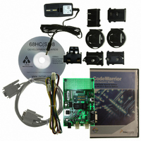
M68EVB908QL4
Description
BOARD EVALUATION FOR 908QL4 MCU
Manufacturer
Freescale Semiconductor
Type
MCUr
Datasheet
1.M68EVB908QL4.pdf
(13 pages)
Specifications of M68EVB908QL4
Contents
Module and Misc Hardware
For Use With/related Products
MC68HC908QL4 Family
Lead Free Status / RoHS Status
Contains lead / RoHS non-compliant


M 6 8 E V B 9 0 8 Q L 4
LIN Connectors and Options
The LIN network connectors (LIN-J1 and LIN-J2) provide a standard pin configuration with a
network option position.
LIN Signal
Option pin
Option pin 2 on the LIN connectors provides an additional ground or Test Pad to apply another
signal with the network. Test pad TP2 provides option access to LIN-J1 and TP3 provides
option access to LIN-J2. Option pad set 1 and 2 will provide connections to ground for LIN_J1
and LIN-J2 option pin 2 respectfully.
MC68HC980QL4 PORT CONNECTORS
MCU_PORT
The MCU PORT provides access to the MC68HC908QL4 I/O ports. Port configuration reflects
the DIP package device pin and signal order.
Notes:
1) PTA0 – 2, PTA4, and PTA5 applied with CYCLONE cable if installed.
2) PTA0 is also the MON08 debug monitor serial I/O (MON_EN).
3) PTA2 provides IRQ Push Switch input (JP1) or Monitor mode entry voltage (MON_EN).
4) PTA3 provides RESET Push Switch input (JP1).
5) PTB0 provides D1 indicator output (JP1).
6) PTB3/AD5 provides RV1 user pot input (JP1).
7) PTB4 provides LIN serial input (SLCRX).
8) PTB5 provides LIN serial output (SLCTX).
PTA2/IRQ*/KBI2/TCLK
PTA1/TCH1/KBI1
PTA3/RST*/KBI3
Front view (looking into connector from outside of board edge)
4
2
PTB0/TCH0
+5V (VDD)
PTB3/AD5
PTB2/AD4
PTB1
3 +VSUP Input
1 Ground
1 16
2 15
3 14
4 13
5 12
6 11
7 10
8 9
GND (VSS)
PTA0/AD0/KBD0
PTA5/OSC1/AD3/KBD5
PTA4/OSC2/AD2/KBI4
PTB4/SLCRX
PTB5/SLCTX
PTB6
PTB7
11
Mating connector = Molex 39-01-2040 with
39-00-0039 pins
1 2 / 0 4 / 0 3
Related parts for M68EVB908QL4
Image
Part Number
Description
Manufacturer
Datasheet
Request
R

Part Number:
Description:
Manufacturer:
Freescale Semiconductor, Inc
Datasheet:
Part Number:
Description:
Manufacturer:
Freescale Semiconductor, Inc
Datasheet:
Part Number:
Description:
Manufacturer:
Freescale Semiconductor, Inc
Datasheet:
Part Number:
Description:
Manufacturer:
Freescale Semiconductor, Inc
Datasheet:
Part Number:
Description:
Manufacturer:
Freescale Semiconductor, Inc
Datasheet:
Part Number:
Description:
Manufacturer:
Freescale Semiconductor, Inc
Datasheet:
Part Number:
Description:
Manufacturer:
Freescale Semiconductor, Inc
Datasheet:
Part Number:
Description:
Manufacturer:
Freescale Semiconductor, Inc
Datasheet:
Part Number:
Description:
Manufacturer:
Freescale Semiconductor, Inc
Datasheet:
Part Number:
Description:
Manufacturer:
Freescale Semiconductor, Inc
Datasheet:
Part Number:
Description:
Manufacturer:
Freescale Semiconductor, Inc
Datasheet:
Part Number:
Description:
Manufacturer:
Freescale Semiconductor, Inc
Datasheet:
Part Number:
Description:
Manufacturer:
Freescale Semiconductor, Inc
Datasheet:
Part Number:
Description:
Manufacturer:
Freescale Semiconductor, Inc
Datasheet:
Part Number:
Description:
Manufacturer:
Freescale Semiconductor, Inc
Datasheet: