C8051T630DK Silicon Laboratories Inc, C8051T630DK Datasheet - Page 13
C8051T630DK
Manufacturer Part Number
C8051T630DK
Description
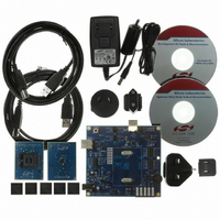
KIT DEV FOR C8051T630 FAMILY
Manufacturer
Silicon Laboratories Inc
Type
MCUr
Specifications of C8051T630DK
Contents
Board, daughter boards, power adapter, cables, documentation and software
Processor To Be Evaluated
C8051T63x
Interface Type
USB
Lead Free Status / RoHS Status
Lead free / RoHS Compliant
For Use With/related Products
C8051T630, T631, T632, T633, T634 and T635 MCUs
For Use With
336-1465 - BOARD SOCKET DAUGHTER 20-QFN
Lead Free Status / Rohs Status
Lead free / RoHS Compliant
Other names
336-1464


7.7. PORT I/O Connectors (J2, J3 and J4)
Each of the C8051T63x's I/O pins, as well as +3VD and GND, are routed to headers J2 through J4. J2 connects to
the microcontroller's Port 0 pins, J3 connects to Port 1, and J4 connects to Port 2.
7.8. Analog I/O (J1)
Three of the C8051T63x target device's port pins are connected to the J1 terminal block. The terminal block also
allows users to input an external voltage that can be used as the power supply of the board. Refer to Table 2 for the
J1 terminal block connections.
7.9. VPP Connection (J11)
The C8051T63x devices require a special 6.5 V programming voltage applied to the VPP pin during device
programming. The VPP pin on these devices is shared with P0.2. During programming, the VPP voltage is
automatically enabled when needed. Header J11 is provided to allow the user to disconnect the programming
circuitry from the VPP/P0.2 pin to avoid interfering with the normal application operation of P0.2. When
programming the device, J11 should be shorted with a shorting block. When running normal application code, J11
can be removed.
7.10. Using Alternate Supplies with the C8051T63x Development Kit
For most evaluation purposes, the onboard 3.3 V supply regulator is sufficient to be used as a VDD power supply.
However, in applications where a different supply voltage is desired (e.g., 1.8 V), an external supply voltage can be
applied to the board at the analog connector (J1).
Notes:
1. When programming a C8051T63x device, the onboard 3.3 V regulator should be used for VDD.
2. If an external supply voltage is desired, the shorting block on J6 should be placed so that the pin 3 (VDD_EXT)
is shorted to pin 4 (VDD_PWR).
Figure 8. Shorting Block Configuration for UART Communication Options
RTS_CP2103
RX_CP2103
(USB Connection at P4)
RTS_F326
RX_F326
CP2103 Bridge
Table 2. J1 Terminal Block Descriptions
P1.1
P0.4
Pin #
J10
1
2
3
4
5
J8
CTS_F326
P1.2
CTS_CP2103
TX_F326
P0.5
TX_CP2103
Rev. 0.1
VDD_EXT (routed to header J6)
RTS_CP2103
RX_CP2103
(USB Connection at P5)
Debug Adapter Comms
RTS_F326
RX_F326
P1.6 (Analog Input)
GND (Ground)
P1.1
P0.4
Description
P0.0/VREF
P0.1/IDAC
J10
J8
CTS_CP2103
CTS_F326
P1.2
TX_F326
P0.5
TX_CP2103
C8051T63x-DK
13
Related parts for C8051T630DK
Image
Part Number
Description
Manufacturer
Datasheet
Request
R

Part Number:
Description:
SMD/C°/SINGLE-ENDED OUTPUT SILICON OSCILLATOR
Manufacturer:
Silicon Laboratories Inc
Part Number:
Description:
Manufacturer:
Silicon Laboratories Inc
Datasheet:
Part Number:
Description:
N/A N/A/SI4010 AES KEYFOB DEMO WITH LCD RX
Manufacturer:
Silicon Laboratories Inc
Datasheet:
Part Number:
Description:
N/A N/A/SI4010 SIMPLIFIED KEY FOB DEMO WITH LED RX
Manufacturer:
Silicon Laboratories Inc
Datasheet:
Part Number:
Description:
N/A/-40 TO 85 OC/EZLINK MODULE; F930/4432 HIGH BAND (REV E/B1)
Manufacturer:
Silicon Laboratories Inc
Part Number:
Description:
EZLink Module; F930/4432 Low Band (rev e/B1)
Manufacturer:
Silicon Laboratories Inc
Part Number:
Description:
I°/4460 10 DBM RADIO TEST CARD 434 MHZ
Manufacturer:
Silicon Laboratories Inc
Part Number:
Description:
I°/4461 14 DBM RADIO TEST CARD 868 MHZ
Manufacturer:
Silicon Laboratories Inc
Part Number:
Description:
I°/4463 20 DBM RFSWITCH RADIO TEST CARD 460 MHZ
Manufacturer:
Silicon Laboratories Inc
Part Number:
Description:
I°/4463 20 DBM RADIO TEST CARD 868 MHZ
Manufacturer:
Silicon Laboratories Inc
Part Number:
Description:
I°/4463 27 DBM RADIO TEST CARD 868 MHZ
Manufacturer:
Silicon Laboratories Inc
Part Number:
Description:
I°/4463 SKYWORKS 30 DBM RADIO TEST CARD 915 MHZ
Manufacturer:
Silicon Laboratories Inc
Part Number:
Description:
N/A N/A/-40 TO 85 OC/4463 RFMD 30 DBM RADIO TEST CARD 915 MHZ
Manufacturer:
Silicon Laboratories Inc
Part Number:
Description:
I°/4463 20 DBM RADIO TEST CARD 169 MHZ
Manufacturer:
Silicon Laboratories Inc