C8051F336DK Silicon Laboratories Inc, C8051F336DK Datasheet - Page 11
C8051F336DK
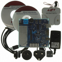
Manufacturer Part Number
C8051F336DK
Description
DEV KIT FOR C8051F336
Manufacturer
Silicon Laboratories Inc
Type
MCUr
Specifications of C8051F336DK
Contents
Evaluation Board, Power Supply, USB Cables, Adapter and Documentation
Processor To Be Evaluated
C8051F33x
Interface Type
USB, UART
Operating Supply Voltage
7 V to 15 V
Lead Free Status / RoHS Status
Lead free / RoHS Compliant
For Use With/related Products
C8051F336
Lead Free Status / Rohs Status
Lead free / RoHS Compliant
Other names
336-1430


8.5. Expansion I/O Connector (J1)
The 26-pin Expansion I/O connector J1 provides access to all signal pins of the C8051F338 device. Pins for +3 V,
digital ground and the output of an on-board low-pass filter are also available. A small through-hole prototyping
area is also provided. All I/O signals routed to connector J1 are also routed to through-hole connection points
between J1 and the prototyping area (see Figure 3 on page 7). Each connection point is labeled indicating the
signal available at the connection point. See Table 2 for a list of pin descriptions for J1.
8.6. Target Board DEBUG Interface (J4)
The DEBUG connector J4 provides access to the DEBUG (C2) pins of the C8051F338. It is used to connect the
Serial Adapter or the USB Debug Adapter to the target board for in-circuit debugging and Flash programming.
Table 3 shows the DEBUG pin definitions.
Pin #
10
11
12
13
Table 3. DEBUG Connector Pin Descriptions
1
2
3
4
5
6
7
8
9
+3 VD (+3.3 VDC)
2, 3, 9
Pin #
10
Description
1
4
5
6
7
8
Table 2. J1 Pin Descriptions
IDAC
P0.0
P0.1
P0.2
P0.3
P0.4
P0.5
P0.6
P0.7
P1.0
P1.1
P1.2
USB Power (+5VDC from J4)
+3 VD (+3.3 VDC)
Rev. 0.2
Not Connected
GND (Ground)
Description
/RST (Reset)
/RST/C2CK
P2.4/C2D
P2.4
Pin #
14
15
16
17
18
19
20
21
22
23
24
25
26
Description
/RST
GND
GND
P1.3
P1.4
P1.5
P1.6
P1.7
P2.0
P2.1
P2.2
P2.3
P2.4
C8051F336DK
11
Related parts for C8051F336DK
Image
Part Number
Description
Manufacturer
Datasheet
Request
R

Part Number:
Description:
SMD/C°/SINGLE-ENDED OUTPUT SILICON OSCILLATOR
Manufacturer:
Silicon Laboratories Inc
Part Number:
Description:
Manufacturer:
Silicon Laboratories Inc
Datasheet:
Part Number:
Description:
N/A N/A/SI4010 AES KEYFOB DEMO WITH LCD RX
Manufacturer:
Silicon Laboratories Inc
Datasheet:
Part Number:
Description:
N/A N/A/SI4010 SIMPLIFIED KEY FOB DEMO WITH LED RX
Manufacturer:
Silicon Laboratories Inc
Datasheet:
Part Number:
Description:
N/A/-40 TO 85 OC/EZLINK MODULE; F930/4432 HIGH BAND (REV E/B1)
Manufacturer:
Silicon Laboratories Inc
Part Number:
Description:
EZLink Module; F930/4432 Low Band (rev e/B1)
Manufacturer:
Silicon Laboratories Inc
Part Number:
Description:
I°/4460 10 DBM RADIO TEST CARD 434 MHZ
Manufacturer:
Silicon Laboratories Inc
Part Number:
Description:
I°/4461 14 DBM RADIO TEST CARD 868 MHZ
Manufacturer:
Silicon Laboratories Inc
Part Number:
Description:
I°/4463 20 DBM RFSWITCH RADIO TEST CARD 460 MHZ
Manufacturer:
Silicon Laboratories Inc
Part Number:
Description:
I°/4463 20 DBM RADIO TEST CARD 868 MHZ
Manufacturer:
Silicon Laboratories Inc
Part Number:
Description:
I°/4463 27 DBM RADIO TEST CARD 868 MHZ
Manufacturer:
Silicon Laboratories Inc
Part Number:
Description:
I°/4463 SKYWORKS 30 DBM RADIO TEST CARD 915 MHZ
Manufacturer:
Silicon Laboratories Inc
Part Number:
Description:
N/A N/A/-40 TO 85 OC/4463 RFMD 30 DBM RADIO TEST CARD 915 MHZ
Manufacturer:
Silicon Laboratories Inc
Part Number:
Description:
I°/4463 20 DBM RADIO TEST CARD 169 MHZ
Manufacturer:
Silicon Laboratories Inc