C8051T600DK Silicon Laboratories Inc, C8051T600DK Datasheet - Page 7
C8051T600DK
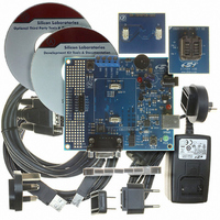
Manufacturer Part Number
C8051T600DK
Description
KIT DEV FOR C8051T60X MCU'S
Manufacturer
Silicon Laboratories Inc
Type
MCUr
Specifications of C8051T600DK
Contents
Evaluation Board, Power Supply, USB Cables, Adapter and Documentation
Processor To Be Evaluated
C8051T60x
Interface Type
USB
Lead Free Status / RoHS Status
Contains lead / RoHS non-compliant
For Use With/related Products
C8051T600, C8051T601, C8051T602, C8051T603, C8051T604, C8051T605
Lead Free Status / Rohs Status
Lead free / RoHS Compliant
Other names
336-1404


13. Comparator0
14. CIP-51 Microcontroller
15. Memory Organization
16. Special Function Registers
17. Interrupts
18. Power Management Modes
19. Reset Sources
20. EPROM Memory
21. Oscillators and Clock Selection
22. Port Input/Output
23. SMBus
24. UART0
25. Timers
Figure 13.1. Comparator0 Functional Block Diagram ............................................. 59
Figure 13.2. Comparator Hysteresis Plot ................................................................ 60
Figure 13.3. Comparator Input Multiplexer Block Diagram ...................................... 63
Figure 14.1. CIP-51 Block Diagram ......................................................................... 65
Figure 15.1. Program Memory Map ......................................................................... 74
Figure 15.2. RAM Memory Map .............................................................................. 75
Figure 19.1. Reset Sources ..................................................................................... 92
Figure 19.2. Power-On and VDD Monitor Reset Timing ......................................... 93
Figure 21.1. Oscillator Options .............................................................................. 100
Figure 22.1. Port I/O Functional Block Diagram .................................................... 106
Figure 22.2. Port I/O Cell Block Diagram .............................................................. 107
Figure 22.3. Priority Crossbar Decoder Potential Pin Assignments ...................... 111
Figure 22.4. Priority Crossbar Decoder Example 1 - No Skipped Pins ................. 112
Figure 22.5. Priority Crossbar Decoder Example 2 - Skipping Pins ...................... 113
Figure 23.1. SMBus Block Diagram ...................................................................... 120
Figure 23.2. Typical SMBus Configuration ............................................................ 121
Figure 23.3. SMBus Transaction ........................................................................... 122
Figure 23.4. Typical SMBus SCL Generation ........................................................ 124
Figure 23.5. Typical Master Write Sequence ........................................................ 131
Figure 23.6. Typical Master Read Sequence ........................................................ 132
Figure 23.7. Typical Slave Write Sequence .......................................................... 133
Figure 23.8. Typical Slave Read Sequence .......................................................... 134
Figure 24.1. UART0 Block Diagram ...................................................................... 137
Figure 24.2. UART0 Baud Rate Logic ................................................................... 138
Figure 24.3. UART Interconnect Diagram ............................................................. 139
Figure 24.4. 8-Bit UART Timing Diagram .............................................................. 139
Figure 24.5. 9-Bit UART Timing Diagram .............................................................. 140
Figure 24.6. UART Multi-Processor Mode Interconnect Diagram ......................... 141
Figure 25.1. T0 Mode 0 Block Diagram ................................................................. 148
Figure 25.2. T0 Mode 2 Block Diagram ................................................................. 149
Figure 25.3. T0 Mode 3 Block Diagram ................................................................. 150
Figure 25.4. Timer 2 16-Bit Mode Block Diagram ................................................. 155
Rev. 1.2
C8051T600/1/2/3/4/5/6
7
Related parts for C8051T600DK
Image
Part Number
Description
Manufacturer
Datasheet
Request
R

Part Number:
Description:
SMD/C°/SINGLE-ENDED OUTPUT SILICON OSCILLATOR
Manufacturer:
Silicon Laboratories Inc
Part Number:
Description:
Manufacturer:
Silicon Laboratories Inc
Datasheet:
Part Number:
Description:
N/A N/A/SI4010 AES KEYFOB DEMO WITH LCD RX
Manufacturer:
Silicon Laboratories Inc
Datasheet:
Part Number:
Description:
N/A N/A/SI4010 SIMPLIFIED KEY FOB DEMO WITH LED RX
Manufacturer:
Silicon Laboratories Inc
Datasheet:
Part Number:
Description:
N/A/-40 TO 85 OC/EZLINK MODULE; F930/4432 HIGH BAND (REV E/B1)
Manufacturer:
Silicon Laboratories Inc
Part Number:
Description:
EZLink Module; F930/4432 Low Band (rev e/B1)
Manufacturer:
Silicon Laboratories Inc
Part Number:
Description:
I°/4460 10 DBM RADIO TEST CARD 434 MHZ
Manufacturer:
Silicon Laboratories Inc
Part Number:
Description:
I°/4461 14 DBM RADIO TEST CARD 868 MHZ
Manufacturer:
Silicon Laboratories Inc
Part Number:
Description:
I°/4463 20 DBM RFSWITCH RADIO TEST CARD 460 MHZ
Manufacturer:
Silicon Laboratories Inc
Part Number:
Description:
I°/4463 20 DBM RADIO TEST CARD 868 MHZ
Manufacturer:
Silicon Laboratories Inc
Part Number:
Description:
I°/4463 27 DBM RADIO TEST CARD 868 MHZ
Manufacturer:
Silicon Laboratories Inc
Part Number:
Description:
I°/4463 SKYWORKS 30 DBM RADIO TEST CARD 915 MHZ
Manufacturer:
Silicon Laboratories Inc
Part Number:
Description:
N/A N/A/-40 TO 85 OC/4463 RFMD 30 DBM RADIO TEST CARD 915 MHZ
Manufacturer:
Silicon Laboratories Inc
Part Number:
Description:
I°/4463 20 DBM RADIO TEST CARD 169 MHZ
Manufacturer:
Silicon Laboratories Inc