C8051T600DK Silicon Laboratories Inc, C8051T600DK Datasheet - Page 113
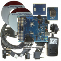
C8051T600DK
Manufacturer Part Number
C8051T600DK
Description
KIT DEV FOR C8051T60X MCU'S
Manufacturer
Silicon Laboratories Inc
Type
MCUr
Specifications of C8051T600DK
Contents
Evaluation Board, Power Supply, USB Cables, Adapter and Documentation
Processor To Be Evaluated
C8051T60x
Interface Type
USB
Lead Free Status / RoHS Status
Contains lead / RoHS non-compliant
For Use With/related Products
C8051T600, C8051T601, C8051T602, C8051T603, C8051T604, C8051T605
Lead Free Status / Rohs Status
Lead free / RoHS Compliant
Other names
336-1404


Registers XBR1 and XBR2 are used to assign the digital I/O resources to the physical I/O Port pins. Note
that when the SMBus is selected, the crossbar assigns both pins associated with the SMBus (SDA and
SCL). UART0 pin assignments are fixed for bootloading purposes: UART TX0 is always assigned to P0.4;
UART RX0 is always assigned to P0.5. Standard Port I/Os appear contiguously after the prioritized func-
tions have been assigned.
SYSCLK
Function
Pin Skip
Settings
Special
Signals
Figure 22.5. Priority Crossbar Decoder Example 2 - Skipping Pins
CP0A
CEX0
CEX1
CEX2
SDA
RX0
SCL
CP0
Port
TX0
ECI
Pin
T0
T1
0 1 2 3 4 5 6 7
1 0 0 1 0 0 0 x
XBR0
P0
In this example, the crossbar is configured to
assign the UART TX0 and RX0 signals, the
SMBus signals, and the SYSCLK signal. Note
that the SMBus signals are assigned as a pair.
Additionally, pins P0.0 and P0.3 are configured
to be skipped using the XBR0 register.
are used by the peripherals in this configuration.
1
2
3
respectively.
4
All unassigned pins, including those skipped by
XBR0 can be used as GPIO or for other non-
crossbar functions.
Rev. 1.2
st
nd
rd
th
TX0 is assigned to P0.4
SYSCLK is assigned to P0.6
SDA and SCL are assigned to P0.2 and P0.3,
RX0 is assigned to P0.5
These boxes represent the port pins which
C8051T600/1/2/3/4/5/6
113
Related parts for C8051T600DK
Image
Part Number
Description
Manufacturer
Datasheet
Request
R

Part Number:
Description:
SMD/C°/SINGLE-ENDED OUTPUT SILICON OSCILLATOR
Manufacturer:
Silicon Laboratories Inc
Part Number:
Description:
Manufacturer:
Silicon Laboratories Inc
Datasheet:
Part Number:
Description:
N/A N/A/SI4010 AES KEYFOB DEMO WITH LCD RX
Manufacturer:
Silicon Laboratories Inc
Datasheet:
Part Number:
Description:
N/A N/A/SI4010 SIMPLIFIED KEY FOB DEMO WITH LED RX
Manufacturer:
Silicon Laboratories Inc
Datasheet:
Part Number:
Description:
N/A/-40 TO 85 OC/EZLINK MODULE; F930/4432 HIGH BAND (REV E/B1)
Manufacturer:
Silicon Laboratories Inc
Part Number:
Description:
EZLink Module; F930/4432 Low Band (rev e/B1)
Manufacturer:
Silicon Laboratories Inc
Part Number:
Description:
I°/4460 10 DBM RADIO TEST CARD 434 MHZ
Manufacturer:
Silicon Laboratories Inc
Part Number:
Description:
I°/4461 14 DBM RADIO TEST CARD 868 MHZ
Manufacturer:
Silicon Laboratories Inc
Part Number:
Description:
I°/4463 20 DBM RFSWITCH RADIO TEST CARD 460 MHZ
Manufacturer:
Silicon Laboratories Inc
Part Number:
Description:
I°/4463 20 DBM RADIO TEST CARD 868 MHZ
Manufacturer:
Silicon Laboratories Inc
Part Number:
Description:
I°/4463 27 DBM RADIO TEST CARD 868 MHZ
Manufacturer:
Silicon Laboratories Inc
Part Number:
Description:
I°/4463 SKYWORKS 30 DBM RADIO TEST CARD 915 MHZ
Manufacturer:
Silicon Laboratories Inc
Part Number:
Description:
N/A N/A/-40 TO 85 OC/4463 RFMD 30 DBM RADIO TEST CARD 915 MHZ
Manufacturer:
Silicon Laboratories Inc
Part Number:
Description:
I°/4463 20 DBM RADIO TEST CARD 169 MHZ
Manufacturer:
Silicon Laboratories Inc