C8051F064EK Silicon Laboratories Inc, C8051F064EK Datasheet - Page 96
C8051F064EK
Manufacturer Part Number
C8051F064EK
Description
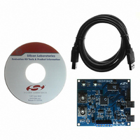
KIT EVAL FOR C8051F064
Manufacturer
Silicon Laboratories Inc
Type
MCUr
Specifications of C8051F064EK
Contents
Evaluation Board, Power Supply, USB Cables, Adapter and Documentation
Processor To Be Evaluated
C8051F06x
Interface Type
USB
Silicon Manufacturer
Silicon Labs
Core Architecture
8051
Silicon Core Number
C8051F064
Silicon Family Name
C8051F06x
Lead Free Status / RoHS Status
Contains lead / RoHS non-compliant
For Use With/related Products
C8051F064
Lead Free Status / Rohs Status
Lead free / RoHS Compliant
Other names
336-1219


C8051F060/1/2/3/4/5/6/7
96
Bit 7:
Bit6:
Bit5:
Bit 4:
Bits 3-2: AD2CM1-0: ADC2 Start of Conversion Mode Select.
Bit 1:
Bit 0:
SFR Page:
SFR Address:
AD2EN
R/W
Bit7
AD2EN: ADC2 Enable Bit.
0: ADC2 Disabled. ADC2 is in low-power shutdown.
1: ADC2 Enabled. ADC2 is active and ready for data conversions.
AD2TM: ADC2 Track Mode Bit.
0: Normal Track Mode: When ADC2 is enabled, tracking is continuous unless a conversion
is in progress.
1: Low-power Track Mode: Tracking Defined by AD2CM2-0 bits (see below).
AD2INT: ADC2 Conversion Complete Interrupt Flag.
0: ADC2 has not completed a data conversion since the last time AD2INT was cleared.
1: ADC2 has completed a data conversion.
AD2BUSY: ADC2 Busy Bit.
Read:
0: ADC2 conversion is complete or a conversion is not currently in progress. AD2INT is set
to logic 1 on the falling edge of AD2BUSY.
1: ADC2 conversion is in progress.
Write:
0: No Effect.
1: Initiates ADC2 Conversion if AD2CM2-0 = 000b
When AD2TM = 0:
00: ADC2 conversion initiated on every write of ‘1’ to AD2BUSY.
01: ADC2 conversion initiated on overflow of Timer 3.
10: ADC2 conversion initiated on rising edge of external CNVSTR2 pin.
11: ADC2 conversion initiated on overflow of Timer 2.
When AD2TM = 1:
00: Tracking initiated on write of ‘1’ to AD2BUSY and lasts 3 SAR clocks, followed by con-
version.
01: Tracking initiated on overflow of Timer 3 and lasts 3 SAR clocks, followed by conver-
sion.
10: ADC2 tracks only when CNVSTR2 input is logic low; conversion starts on rising
CNVSTR2 edge.
11: Tracking initiated on overflow of Timer 2 and lasts 3 SAR clocks, followed by conversion.
AD2WINT: ADC2 Window Compare Interrupt Flag.
0: ADC2 Window Comparison Data match has not occurred since this flag was last cleared.
1: ADC2 Window Comparison Data match has occurred.
AD2LJST: ADC2 Left Justify Select.
0: Data in ADC2H:ADC2L registers are right-justified.
1: Data in ADC2H:ADC2L registers are left-justified.
2
0xE8
AD2TM
R/W
Bit6
(bit addressable)
AD2INT
R/W
Figure 7.10. ADC2CN: ADC2 Control Register
Bit5
AD2BUSY
R/W
Bit4
AD2CM1
Rev. 1.2
R/W
Bit3
AD2CM0
R/W
Bit2
AD2WINT
R/W
Bit1
AD2LJST
R/W
Bit0
Reset Value
00000000
Related parts for C8051F064EK
Image
Part Number
Description
Manufacturer
Datasheet
Request
R

Part Number:
Description:
SMD/C°/SINGLE-ENDED OUTPUT SILICON OSCILLATOR
Manufacturer:
Silicon Laboratories Inc
Part Number:
Description:
Manufacturer:
Silicon Laboratories Inc
Datasheet:
Part Number:
Description:
N/A N/A/SI4010 AES KEYFOB DEMO WITH LCD RX
Manufacturer:
Silicon Laboratories Inc
Datasheet:
Part Number:
Description:
N/A N/A/SI4010 SIMPLIFIED KEY FOB DEMO WITH LED RX
Manufacturer:
Silicon Laboratories Inc
Datasheet:
Part Number:
Description:
N/A/-40 TO 85 OC/EZLINK MODULE; F930/4432 HIGH BAND (REV E/B1)
Manufacturer:
Silicon Laboratories Inc
Part Number:
Description:
EZLink Module; F930/4432 Low Band (rev e/B1)
Manufacturer:
Silicon Laboratories Inc
Part Number:
Description:
I°/4460 10 DBM RADIO TEST CARD 434 MHZ
Manufacturer:
Silicon Laboratories Inc
Part Number:
Description:
I°/4461 14 DBM RADIO TEST CARD 868 MHZ
Manufacturer:
Silicon Laboratories Inc
Part Number:
Description:
I°/4463 20 DBM RFSWITCH RADIO TEST CARD 460 MHZ
Manufacturer:
Silicon Laboratories Inc
Part Number:
Description:
I°/4463 20 DBM RADIO TEST CARD 868 MHZ
Manufacturer:
Silicon Laboratories Inc
Part Number:
Description:
I°/4463 27 DBM RADIO TEST CARD 868 MHZ
Manufacturer:
Silicon Laboratories Inc
Part Number:
Description:
I°/4463 SKYWORKS 30 DBM RADIO TEST CARD 915 MHZ
Manufacturer:
Silicon Laboratories Inc
Part Number:
Description:
N/A N/A/-40 TO 85 OC/4463 RFMD 30 DBM RADIO TEST CARD 915 MHZ
Manufacturer:
Silicon Laboratories Inc
Part Number:
Description:
I°/4463 20 DBM RADIO TEST CARD 169 MHZ
Manufacturer:
Silicon Laboratories Inc