C8051F226DK Silicon Laboratories Inc, C8051F226DK Datasheet - Page 25
C8051F226DK
Manufacturer Part Number
C8051F226DK
Description
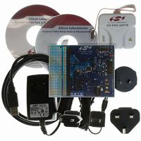
DEV KIT F220/221/226/230/231/236
Manufacturer
Silicon Laboratories Inc
Type
MCUr
Datasheet
1.C8051F226DK.pdf
(146 pages)
Specifications of C8051F226DK
Contents
Evaluation Board, Power Supply, USB Cables, Adapter and Documentation
Processor To Be Evaluated
C8051F22x and C8051F23x
Interface Type
USB
Silicon Manufacturer
Silicon Labs
Core Architecture
8051
Silicon Core Number
C8051F226
Silicon Family Name
C8051F2xx
Lead Free Status / RoHS Status
Contains lead / RoHS non-compliant
For Use With/related Products
C8051F220, 221, 226, 230, 231, 236
Lead Free Status / Rohs Status
Lead free / RoHS Compliant
Other names
336-1241


4.
P0.2/INT0
MONEN
P0.1/RX
P0.0/TX
XTAL1
XTAL2
Name
VREF
CP0+
CP1+
CP0-
CP1-
GND
TMS
TDO
TCK
RST
CP0
CP1
V
TDI
Pinout and Package Definitions
DD
48-Pin 32-Pin
5,6,8,
13,32
11,31
‘F206,
F220,
226,
230,
236
12
25
26
28
27
10
14
48
47
40
39
38
9
7
4
3
2
1
‘F221,
231
17
18
20
19
10
32
31
28
27
26
8
9
6
7
5
4
3
2
1
D Out JTAG Test Data Output. Data is shifted out on TDO on the falling
A Out
D Out
D Out
D I/O
A I/O
D I/O
D I/O
D I/O
Type
D In
D In
D In
D In
A In
A In
A In
A In
A In
A In
A In
A In
Table 4.1. Pin Definitions
connected (NC), but it is recommended that they be connected to
tor. Is driven low when V
voltage reference for the ADC. Otherwise, V
XTAL2. If overdriven by an external CMOS clock, this becomes
Chip Reset. Open-drain output of internal Voltage Supply moni-
Voltage Reference. When configured as an input, this pin is the
Crystal Input. This pin is the return for the internal oscillator cir-
Ground. ( Note: Pins 5,6, and 8 on the 48-pin package are not
Monitor Enable (on 48 pin package ONLY). Enables reset volt-
Port0 Bit0. (See the Port I/O Sub-System section for complete
Port0 Bit1. (See the Port I/O Sub-System section for complete
Port0 Bit2. (See the Port I/O Sub-System section for complete
JTAG Test Data Input with internal pull-up. TDI is latched on a
‘1’is written to PORSF. An external source can force a system
cuit for a crystal or ceramic resonator. For a precision internal
Crystal Output. This pin is the excitation driver for a crystal or
clock, connect a crystal or ceramic resonator from XTAL1 to
ence. NOTE: this pin is Not Connected (NC) on ‘F230/1/6.
age monitor function when pulled high (logic “1”).
Rev. 1.6
edge of TCK. TDO output is a tri-state driver.
JTAG Test-Mode Select with internal pull-up.
JTAG Test Clock with internal pull-up.
Comparator 0 Non-Inverting Input.
Comparator 1 Non-Inverting Input.
Comparator 0 Inverting Input.
Comparator 1 Inverting Input.
reset by driving this pin low.
Digital Voltage Supply.
Comparator 0 Output
Comparator 1 Output
rising edge of TCK.
ceramic resonator.
the system clock.
DD
Description
description).
description).
description).
ground.)
is < 2.7V and MONEN=1, or when a
C8051F2xx
DD
will be the refer-
25
Related parts for C8051F226DK
Image
Part Number
Description
Manufacturer
Datasheet
Request
R

Part Number:
Description:
SMD/C°/SINGLE-ENDED OUTPUT SILICON OSCILLATOR
Manufacturer:
Silicon Laboratories Inc
Part Number:
Description:
Manufacturer:
Silicon Laboratories Inc
Datasheet:
Part Number:
Description:
N/A N/A/SI4010 AES KEYFOB DEMO WITH LCD RX
Manufacturer:
Silicon Laboratories Inc
Datasheet:
Part Number:
Description:
N/A N/A/SI4010 SIMPLIFIED KEY FOB DEMO WITH LED RX
Manufacturer:
Silicon Laboratories Inc
Datasheet:
Part Number:
Description:
N/A/-40 TO 85 OC/EZLINK MODULE; F930/4432 HIGH BAND (REV E/B1)
Manufacturer:
Silicon Laboratories Inc
Part Number:
Description:
EZLink Module; F930/4432 Low Band (rev e/B1)
Manufacturer:
Silicon Laboratories Inc
Part Number:
Description:
I°/4460 10 DBM RADIO TEST CARD 434 MHZ
Manufacturer:
Silicon Laboratories Inc
Part Number:
Description:
I°/4461 14 DBM RADIO TEST CARD 868 MHZ
Manufacturer:
Silicon Laboratories Inc
Part Number:
Description:
I°/4463 20 DBM RFSWITCH RADIO TEST CARD 460 MHZ
Manufacturer:
Silicon Laboratories Inc
Part Number:
Description:
I°/4463 20 DBM RADIO TEST CARD 868 MHZ
Manufacturer:
Silicon Laboratories Inc
Part Number:
Description:
I°/4463 27 DBM RADIO TEST CARD 868 MHZ
Manufacturer:
Silicon Laboratories Inc
Part Number:
Description:
I°/4463 SKYWORKS 30 DBM RADIO TEST CARD 915 MHZ
Manufacturer:
Silicon Laboratories Inc
Part Number:
Description:
N/A N/A/-40 TO 85 OC/4463 RFMD 30 DBM RADIO TEST CARD 915 MHZ
Manufacturer:
Silicon Laboratories Inc
Part Number:
Description:
I°/4463 20 DBM RADIO TEST CARD 169 MHZ
Manufacturer:
Silicon Laboratories Inc