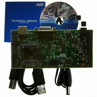
ATSTK526 Atmel, ATSTK526 Datasheet - Page 10
ATSTK526
Manufacturer Part Number
ATSTK526
Description
KIT STARTER FOR AT90USB82/162
Manufacturer
Atmel
Series
AVR®r
Type
MCUr
Specifications of ATSTK526
Contents
Starter Kit Board, Power Supply, Cable and Software
Processor To Be Evaluated
AT90USB82/162
Data Bus Width
8 bit
Interface Type
RS-232, USB
Silicon Manufacturer
Atmel
Core Architecture
AVR
Silicon Core Number
AT90USB82, AT90USB162
Kit Contents
Board Docs
Rohs Compliant
Yes
For Use With/related Products
AT90USB162, AT90USB82
For Use With
ATSTK500 - PROGRAMMER AVR STARTER KIT
Lead Free Status / RoHS Status
Lead free / RoHS Compliant


2.2.3
STK526 rev. B Hardware User Guide
Jumper position
“3V3 REG”
“INTREG”
“NOREG”
AT90USB82/162 Power Configuration Settings
Primary power source
Internal regulator
AT90USB16 I/O power supply
This section applies to the following part of the power path diagram :
Figure 2-5 . MCU Power Configurations
Once the power source selected, the input of the AT90USB82/162 internal regulator
(UVcc) is powered. Firmware has the responsability to enable or disable the regulator.
Ucap is the output pin of the internal regulator, and Vcc is the core power input of the
MCU. Several cases may be required by the user :
Table 2-2 . MCU Power Configuration Jumpers
Vsource = 5V, Vcc = 5V: for this mode, the configuration switch (see figure above)
must be in the position labelled “NOREG”. The MCU can still run a USB Device
application if it enables the internal regulator that will power the USB pad and macro.
Vsource = 5V, Vcc = 3.3V: for this mode, the configuration switch must be in the
position labelled “INTREG”. The Vcc pin will be tied to the regulator output, so that
the AT90USB82/162 itself will power itself from its regulator, and the I/O will be at
3V3 level.
Vsource = 3.3V, Vcc = 3.3V: for this mode all the MCU power inputs are at the 3V3
level. The configuration switch must be in the position “NOREG”. In normal operation
it is recommended to tie all the power pins together (UVcc, Vcc, Ucap) and to disable
the regulator. However, the board configuration does not allow to tie together all the
power pins, so that the regulator must be enabled by firmware in order to power the
USB pad and macro (that can lead to some extra-consumption).
)
This is the default configuration.
This configuration is relevant with a
5V primary powered application
requiring I/O levels at 3.3V on the
AT90USB82/162.
Vsource
Comments
NOREG
Internal
3V3 100mA
Regulator
(1)
(3V3 REG)
(2)
INTREG
AT90USBxx2
1µF
3V3 REG
3V3 REG
View
Using the STK526
7709B–AVR–07/08
2-9
Related parts for ATSTK526
Image
Part Number
Description
Manufacturer
Datasheet
Request
R

Part Number:
Description:
DEV KIT FOR AVR/AVR32
Manufacturer:
Atmel
Datasheet:

Part Number:
Description:
INTERVAL AND WIPE/WASH WIPER CONTROL IC WITH DELAY
Manufacturer:
ATMEL Corporation
Datasheet:
Part Number:
Description:
Low-Voltage Voice-Switched IC for Hands-Free Operation
Manufacturer:
ATMEL Corporation
Datasheet:
Part Number:
Description:
MONOLITHIC INTEGRATED FEATUREPHONE CIRCUIT
Manufacturer:
ATMEL Corporation
Datasheet:
Part Number:
Description:
AM-FM Receiver IC U4255BM-M
Manufacturer:
ATMEL Corporation
Datasheet:
Part Number:
Description:
Monolithic Integrated Feature Phone Circuit
Manufacturer:
ATMEL Corporation
Datasheet:
Part Number:
Description:
Multistandard Video-IF and Quasi Parallel Sound Processing
Manufacturer:
ATMEL Corporation
Datasheet:
Part Number:
Description:
High-performance EE PLD
Manufacturer:
ATMEL Corporation
Datasheet:
Part Number:
Description:
8-bit Flash Microcontroller
Manufacturer:
ATMEL Corporation
Datasheet:
Part Number:
Description:
2-Wire Serial EEPROM
Manufacturer:
ATMEL Corporation
Datasheet: