ATF15XX-DK3 Atmel, ATF15XX-DK3 Datasheet - Page 33
ATF15XX-DK3
Manufacturer Part Number
ATF15XX-DK3
Description
KIT DEV FOR ATF15XX CPLD'S
Manufacturer
Atmel
Series
Logic Doubling®r
Type
CPLDr
Specifications of ATF15XX-DK3
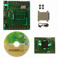
Contents
CPLD Programmer Board, 44-TQFP, Socket Adapter Board, Download Cable, CD-ROMs. Samples and User Guide
Processor To Be Evaluated
ATF15xx
Interface Type
JTAG
Operating Supply Voltage
1.8 V, 3.3 V, 5 V
For Use With/related Products
ATF15xx Family of CPLD
For Use With
ATF15XXDK3-SAJ84 - ADAPTER SKT ATF15XXBE 84/84PLCCATF15XXDK3-SAA100 - ADAPTER SKT ATF15XXB PLCC/TQFPATF15XXDK3-SAJ44 - ADAPTER SKT ATF15XXBE 84/44PLCC
Lead Free Status / RoHS Status
Contains lead / RoHS non-compliant


3605B–PLD–05/06
CPLD Design Flow Tutorial
3-12
The next step requires you to setup the Atmel ATF15xx-DK3 CPLD Development/Pro-
grammer Board to program the ATF1502BE-7AU44 through the CPLD ISP cable.
7. Connect the DB25 side of the Atmel CPLD ISP MV cable (Revision 6) to the PC’s
8. Connect a 9V AC/DC power supply to the power connector (JPower) of the Atmel
9. Set the VCCIO Selector jumper to the 1.8V(BE) position for supplying the core
Note:
10. Set the JPCLK jumper to GCLK1 so that the output of the crystal oscillator will go
11. Set the JPJTAG Jumper ISP Cable position, which is toward the middle of the
12. Connect the 44-pin TQFP Socket Adapter Board onto the main develop-
Note:
13. Select which LPT port is being used for Atmel CPLD ISP cable in the Port Setting
14. Select the ISP download cable type in the Cable Type field. The default cable
Note:
15. Switch the power switch to the ON position.
JEDEC file. Click OK to close the JTAG Device Properties window when all prop-
erties are specified.
parallel port and the 10-pin header side of the cable to the Atmel ATF15xx-DK3
CPLD Development Board as shown Figure 2-10 on page 2-14.
ATF15xx-DK3 CPLD Development/Programmer Board.
voltage of the ATF1502BE device at 1.8V, then set the VCCINT Selector jumper
to the 1.8V(BE) position for supplying the I/O pad voltage of the ATF1502BE
device at 1.8V.
to pin 37 (GCLK1) of the ATF1502BE. For this design, you can also set the
JPCLK jumper to GCLK2 so that the output of the crystal oscillator will go to pin
40 (GCLK2) of the ATF1502BE for selecting another global clock source.
board.
ment/programmer board.
field. LPT1 is the default port and it represents address 0x378.
type is the “Atmel CPLD-ISP MV”, which represents the Atmel CPLD ISP Cable
Rev 6.0, but it can be changed to other cables that can be used for other devices.
Make sure the ICCINT and ICCIO jumpers are in their default positions. These
two jumpers are only removed when you are connecting them from two poles of
the digital multimeter to perform current measurement.
If a device in a different package type is to be programmed, then the appropri-
ate Socket Adapter Board must be used.
The “Atmel CPLD-ISP” cable type represents the Atmel CPLD ISP Cable Rev
5.0 or older.
(4) Specify target
(5) Specify JTAG
(6) Select JEDEC
device type
instruction
file
ATF15xx-DK3 Development Kit User Guide
Related parts for ATF15XX-DK3
Image
Part Number
Description
Manufacturer
Datasheet
Request
R

Part Number:
Description:
ADAPTER FOR ATF15XX-DK2 44TQFP
Manufacturer:
Atmel
Datasheet:
Part Number:
Description:
ADAPTER FOR ATF15XX-DK2 44PLCC
Manufacturer:
Atmel
Datasheet:
Part Number:
Description:
ADAPTER FOR ATF15XX-DK2 68PLCC
Manufacturer:
Atmel
Datasheet:
Part Number:
Description:
ADAPTER FOR ATF15XX-DK2 100TQFP
Manufacturer:
Atmel
Datasheet:
Part Number:
Description:
ADAPTER FOR ATF15XX-DK2 100PQFP
Manufacturer:
Atmel
Datasheet:
Part Number:
Description:
ADAPTER FOR ATF15XX-DK2 160PQFP
Manufacturer:
Atmel
Datasheet:
Part Number:
Description:
DEVELOPMENT KIT CPLD
Manufacturer:
Atmel
Datasheet:
Part Number:
Description:
KIT CPLD DEVELOPMENT/PROGRAMMER
Manufacturer:
Atmel
Datasheet:
Part Number:
Description:
Adapter Skt Atf15xxbe 84/44plcc
Manufacturer:
Atmel
Datasheet:

Part Number:
Description:
DEV KIT FOR AVR/AVR32
Manufacturer:
Atmel
Datasheet:

Part Number:
Description:
INTERVAL AND WIPE/WASH WIPER CONTROL IC WITH DELAY
Manufacturer:
ATMEL Corporation
Datasheet:
Part Number:
Description:
Low-Voltage Voice-Switched IC for Hands-Free Operation
Manufacturer:
ATMEL Corporation
Datasheet:
Part Number:
Description:
MONOLITHIC INTEGRATED FEATUREPHONE CIRCUIT
Manufacturer:
ATMEL Corporation
Datasheet:
Part Number:
Description:
AM-FM Receiver IC U4255BM-M
Manufacturer:
ATMEL Corporation
Datasheet: