HW-SD1800A-DSP-SB-UNI-G Xilinx Inc, HW-SD1800A-DSP-SB-UNI-G Datasheet - Page 21
HW-SD1800A-DSP-SB-UNI-G
Manufacturer Part Number
HW-SD1800A-DSP-SB-UNI-G
Description
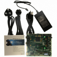
KIT DEVELOPMENT SPARTAN 3ADSP
Manufacturer
Xilinx Inc
Series
Spartan™-3A DSPr
Type
DSPr
Datasheet
1.HW-SD1800A-DSP-SB-UNI-G.pdf
(38 pages)
Specifications of HW-SD1800A-DSP-SB-UNI-G
Contents
Development Platform, Power Supply and software
Silicon Manufacturer
Xilinx
Features
10/100/1000 PHY, JTAG Programming And Configuration Port
Silicon Family Name
Spartan-3A
Silicon Core Number
3SD1800A-FG676
Lead Free Status / RoHS Status
Lead free / RoHS Compliant
For Use With/related Products
Spartan 3A
Lead Free Status / RoHS Status
Lead free / RoHS Compliant, Lead free / RoHS Compliant
Other names
122-1574
HW-SD1800A-DSP-DB-UNI-G
HW-SD1800A-DSP-DB-UNI-G
HW-SD1800A-DSP-SB-UNI-G
HW-SD1800A-DSP-DB-UNI-G
HW-SD1800A-DSP-DB-UNI-G
HW-SD1800A-DSP-SB-UNI-G
Available stocks
Company
Part Number
Manufacturer
Quantity
Price


Table 13: VGA Pin Assignments
Spartan-3A DSP Starter Platform User Guide
UG454 (v1.1) January 30, 2009
R
VGA Output
Table 12: Debug Connector (J3)
The Spartan-3A DSP Starter Platform includes a VGA video output using a resistor-divider
network and 4-bits per RGB color as shown in
510, 1K, 2K, & 4K ohms for each color. The outputs of the three resistor-divider networks
are presented to DB15 connector P1. Horizontal and Vertical synchronization signals are
also generated by the FPGA and provided to P1. Additionally, a 25.175 MHz clock (VGA-
resolution) is added to the board, feeding directly to the FPGA at RHCLK2 (P26) on Bank
1. This clock should be used in the FPGA controller for timing the output and generating
the image and syncs. The VGA pin assignments are listed in
X-Ref Target - Figure 7
J3 Pin Number
VGA Signal
Spartan
3A DSP
FPGA
DAC_G0
DAC_G1
DAC_G2
DAC_G3
DAC_B0
DAC_B1
4
5
6
7
DAC_G [0:3]
DAC_B [0:3]
DAC_R [0:3]
www.xilinx.com
FPGA Pin
M19
M18
K21
L22
J23
J22
Figure 7: VGA Output
Resistor-Divider
Resistor-Divider
Resistor-Divider
Signal Name
DAC_HSYNC
DAC_VSYNC
DBG_Rx_n
DBG_Rx_p
Network
Network
Network
GND
GND
Figure
DAC_HSYNC
DAC_VSYNC
VGA Signal
DAC_R0
DAC_R1
DAC_R2
DAC_R3
7. This resistor-divider network is
Green (analog)
Blue (analog)
Red (analog)
Table
Functional Description
13.
FPGA Pin
FPGA Pin
J20
J10
K20
K25
K26
L20
F25
F24
—
—
DB15
UG454_07_050908
(P1)
45
Related parts for HW-SD1800A-DSP-SB-UNI-G
Image
Part Number
Description
Manufacturer
Datasheet
Request
R

Part Number:
Description:
KIT DEVELOPMENT SPARTAN 3ADSP
Manufacturer:
Xilinx Inc

Part Number:
Description:
IC CPLD .8K 36MCELL 44-VQFP
Manufacturer:
Xilinx Inc
Datasheet:

Part Number:
Description:
IC CPLD 72MCRCELL 10NS 44VQFP
Manufacturer:
Xilinx Inc
Datasheet:

Part Number:
Description:
IC CPLD 1.6K 72MCELL 64-VQFP
Manufacturer:
Xilinx Inc
Datasheet:

Part Number:
Description:
IC CR-II CPLD 64MCELL 44-VQFP
Manufacturer:
Xilinx Inc
Datasheet:

Part Number:
Description:
IC CPLD 1.6K 72MCELL 100-TQFP
Manufacturer:
Xilinx Inc
Datasheet:

Part Number:
Description:
IC CR-II CPLD 64MCELL 56-BGA
Manufacturer:
Xilinx Inc
Datasheet:

Part Number:
Description:
IC CPLD 72MCRCELL 7.5NS 44VQFP
Manufacturer:
Xilinx Inc
Datasheet:
Part Number:
Description:
IC CR-II CPLD 64MCELL 100-VQFP
Manufacturer:
Xilinx Inc
Datasheet:
Part Number:
Description:
IC CPLD 1.6K 72MCELL 100-TQFP
Manufacturer:
Xilinx Inc
Datasheet:

Part Number:
Description:
IC CPLD 72MCRCELL 7.5NS 64VQFP
Manufacturer:
Xilinx Inc
Datasheet:
Part Number:
Description:
IC CPLD 1.6K 72MCELL 100-TQFP
Manufacturer:
Xilinx Inc
Datasheet:

Part Number:
Description:
IC CPLD 1.5K 64MCELL HP 44-VQFP
Manufacturer:
Xilinx Inc

Part Number:
Description:
IC CPLD 36MCRCELL 15NS 44PLCC
Manufacturer:
Xilinx Inc
Datasheet:

Part Number:
Description:
IC CPLD 36MCRCELL 10NS 44PLCC
Manufacturer:
Xilinx Inc
Datasheet: