DK-N2EVAL-3C25N Altera, DK-N2EVAL-3C25N Datasheet - Page 24
DK-N2EVAL-3C25N
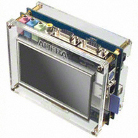
Manufacturer Part Number
DK-N2EVAL-3C25N
Description
KIT DEV NIOS II CYCLONE III ED.
Manufacturer
Altera
Series
Cyclone® IIIr
Type
FPGAr
Specifications of DK-N2EVAL-3C25N
Contents
Development Board, Module, and Software
Silicon Manufacturer
Altera
Core Architecture
FPGA
Core Sub-architecture
Cyclone
Silicon Core Number
EP3C
Silicon Family Name
Cyclone III
Rohs Compliant
Yes
For Use With/related Products
EP3C25
Lead Free Status / RoHS Status
Lead free / RoHS Compliant
Other names
544-2411
DK-N2EVAL-3C25N-OB
DK-NIOSEVAL-3C25N
NEEK
DK-N2EVAL-3C25N-OB
DK-NIOSEVAL-3C25N
NEEK
Available stocks
Company
Part Number
Manufacturer
Quantity
Price


Measuring Power
Measuring
Power
4–2
Cyclone III FPGA Starter Kit User Guide
Table 4–3. LEDs Power State (Resources)
Resources
Displays
f
The design used for power measurement is a replicated set of randomly
filled ROMs that feed a multiplier block and a shift register that is fed by
a signal that changes every clock cycle.
power state which represent the percent of the full design used. As
compiled, this full design uses:
■
■
■
■
■
■
■
■
The example design is located in
<kit install>\examples\cycloneIII_3c25_start_power_demo. Configure
the FPGA with the .sof found in the directory.
1
For more information on configuring the FPGA, refer to
the FPGA Using the Quartus II Programmer” on page
Current sense resistors (0.010 ± 1%) are installed at locations JP6 (FPGA
core power) and JP3 (FPGA I/O power + other device I/O power). With
a digital multimeter set to mV measurement range, the resistor at location
JP6 measures the core power. The resistor at location JP3 measures the
I/O power. To measure the current being used in various configurations,
use the following steps:
LED4
MSB
Logic elements: 22,493/24,624 (91%)
Combinational functions: 1,961/24,624 (8%)
Dedicated logic registers: 21,133/24,624 (86%)
Total registers: 21,133
Total pins: 73/216 (34%)
Total memory bits: 524,288/608,256 (86%)
Embedded Multiplier 9-bit elements: 128/132 (97 %)
Total PLLs: 1/4 (25%)
The input clock (i_clk PIN_B9) is the 50-MHz oscillator on the
board, which generates the input clock for the reference design
through a PLL
LEDs
LED3
LSB
Tables 4–2
State
00
01
10
11
and
2–3.
Altera Corporation
% of Design Used
4–3
“Configuring
show the
100%
25%
50%
75%
July 2010
Related parts for DK-N2EVAL-3C25N
Image
Part Number
Description
Manufacturer
Datasheet
Request
R

Part Number:
Description:
CYCLONE II STARTER KIT EP2C20N
Manufacturer:
Altera
Datasheet:


Part Number:
Description:
CPLD, EP610 Family, ECMOS Process, 300 Gates, 16 Macro Cells, 16 Reg., 16 User I/Os, 5V Supply, 35 Speed Grade, 24DIP
Manufacturer:
Altera Corporation
Datasheet:
Part Number:
Description:
CPLD, EP610 Family, ECMOS Process, 300 Gates, 16 Macro Cells, 16 Reg., 16 User I/Os, 5V Supply, 15 Speed Grade, 24DIP
Manufacturer:
Altera Corporation
Datasheet:
Part Number:
Description:
Manufacturer:
Altera Corporation
Datasheet:
Part Number:
Description:
CPLD, EP610 Family, ECMOS Process, 300 Gates, 16 Macro Cells, 16 Reg., 16 User I/Os, 5V Supply, 30 Speed Grade, 24DIP
Manufacturer:
Altera Corporation
Datasheet:
Part Number:
Description:
High-performance, low-power erasable programmable logic devices with 8 macrocells, 10ns
Manufacturer:
Altera Corporation
Datasheet:
Part Number:
Description:
High-performance, low-power erasable programmable logic devices with 8 macrocells, 7ns
Manufacturer:
Altera Corporation
Datasheet:
Part Number:
Description:
Classic EPLD
Manufacturer:
Altera Corporation
Datasheet:
Part Number:
Description:
High-performance, low-power erasable programmable logic devices with 8 macrocells, 10ns
Manufacturer:
Altera Corporation
Datasheet:
Part Number:
Description:
Manufacturer:
Altera Corporation
Datasheet:
Part Number:
Description:
Manufacturer:
Altera Corporation
Datasheet:
Part Number:
Description:
Manufacturer:
Altera Corporation
Datasheet:
Part Number:
Description:
CPLD, EP610 Family, ECMOS Process, 300 Gates, 16 Macro Cells, 16 Reg., 16 User I/Os, 5V Supply, 25 Speed Grade, 24DIP
Manufacturer:
Altera Corporation
Datasheet: