DK-N2EVAL-3C25N Altera, DK-N2EVAL-3C25N Datasheet
DK-N2EVAL-3C25N
Specifications of DK-N2EVAL-3C25N
DK-N2EVAL-3C25N-OB
DK-NIOSEVAL-3C25N
NEEK
Available stocks


Related parts for DK-N2EVAL-3C25N


DK-N2EVAL-3C25N Summary of contents
Page 1
... Innovation Drive San Jose, CA 95134 www.altera.com P25-36228-03 Cyclone III FPGA Starter Kit User Guide Document Version: Document Date: July 2010 1.2 ...
Page 2
... Altera Corporation. All rights reserved. ALTERA, ARRIA, CYCLONE, HARDCOPY, MAX, MEGACORE, NIOS, QUARTUS and STRATIX are Reg. U.S. Pat. & Tm. Off. and/or trademarks of Altera Corporation in the U.S. and other countries. All other trademarks and service marks are the property of their respective holders as described at www.altera.com/common/legal.html. Altera warrants performance of its semiconductor products to current specifications in accordance with Altera's standard warranty, but reserves the right to make changes to any products and services at any time without notice ...
Page 3
... DDR SDRAM/ SSRAM/On-Chip Controller ............................................................................................................... 3–3 Read/Write Data .............................................................................................................................. 3–4 Read from a File ................................................................................................................................ 3–5 Write to a File ................................................................................................................................... 3–5 Flash Memory Programmer ................................................................................................................. 3–5 Flash Memory Tab ........................................................................................................................... 3–6 CFI Query .......................................................................................................................................... 3–6 Read/Write Data .............................................................................................................................. 3–7 Altera Corporation Contents Cyclone III FPGA Starter Kit User Guide iii ...
Page 4
... Appendix A. Programming the Configuration Flash Device Overview ................................................................................................................................................ A–1 Creating a Flash-Programmable POF File ........................................................................................ A–1 Programming the Flash Device .......................................................................................................... A–5 Additional Information Revision History ............................................................................................................................... Info–i How to Contact Altera .................................................................................................................... Info–ii Typographic Conventions .............................................................................................................. Info–ii iv Cyclone III FPGA Starter Kit User Guide Altera Corporation ...
Page 5
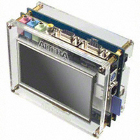
... FPGA development. The development board includes an Altera Cyclone III FPGA and comes preconfigured with a hardware reference design stored in flash memory. You can use the development board as a platform to prototype a variety of FPGA designs ...
Page 6
... Before You Before proceeding, check the contents of the kit: Begin ■ ■ ■ f For the most up-to-date information on this product, visit the Altera website at starter.html. Further For other related information, refer to the following websites: Information For More Information About Additional daughter cards ...
Page 7
... Altera Corporation July 2010 Follow the on-screen instructions to complete the installation process. Figure <install dir> The default Windows installation directory is C:\altera\ <version> \. kits cycloneIII_3c25_start board_design_files demos documents examples factory_recovery lists the file directory names and a description of their contents. ...
Page 8
... Software Installation Installing the Quartus II Web Edition Software The Quartus II Web Edition software provides the necessary tools for developing hardware and software for Altera FPGAs. Included in the Quartus II Web Edition software are the Quartus II software, the Nios II EDS, and the MegaCore SOPC Builder) and the Nios II EDS are the primary FPGA development tools for creating the reference designs in this kit ...
Page 9
... AN 320: OpenCore Plus Evaluation of Nios II Embedded Design Suite (EDS) ® allows you to develop embedded software for the Nios II processor which you can include in your Altera FPGA designs. Cyclone III FPGA Starter Kit User Guide Getting Started Megafunctions. — A full-featured tool set that ...
Page 10
... Software Installation 1–6 Cyclone III FPGA Starter Kit User Guide Altera Corporation July 2010 ...
Page 11
... Connector (J3) Flash LED USB UART (U8) JTAG Header (J4) 32-Mbyte DDR SDRAM (U4) Altera Corporation July 2010 2. Development Board and Control Panel Setup ® III device and board features. At power-up, shows the Cyclone III development board layout and Sense Resistor for FPGA Core Power Measurement (JP6) ...
Page 12
... Installation instructions for the USB-Blaster driver are available on the Altera website at dri-index.html. On the “Altera Programming Cable Driver Information” page of the Altera website, locate the table entry for your configuration and click the link to access the instructions. 2–2 Cyclone III FPGA Starter Kit User Guide ® ...
Page 13
... JTAG chain are Programmer running. To configure the Cyclone III FPGA, follow these steps Altera Corporation July 2010 Development Board and Control Panel Setup Configuring the FPGA Starting the control panel Power up the board and ensure that is is operational. chapter. Start the Quartus II Programmer. ...
Page 14
... Configuring the FPGA Using the Quartus II Programmer 2–4 Cyclone III FPGA Starter Kit User Guide Altera Corporation July 2010 ...
Page 15
... Cyclone III FPGA upon Start power-up with the standard Nios II design. 1 Altera Corporation July 2010 3. Using the Control Panel The graphical user interface (GUI) application on the host computer The standard Nios II hardware design running on the board's ...
Page 16
... The LED & Buttons tab should be visible when the application runs not visible, click the LED & Buttons tab Click on LEDs to individually turn on the LEDs. (Figure 3–1). (Figure 3–2). Altera Corporation July 2010 ...
Page 17
... SSRAM/On-Chip ■ Controller ■ ■ Altera Corporation July 2010 Press the push-button switches on the board. Notice that buttons on the GUI change accordingly. Read from and write to the DDR SDRAM, SSRAM, or on-chip device Write entire contents of a file, to the DDR SDRAM, SSRAM, or ...
Page 18
... C-F columns are the DDR SDRAM contents in hex words format. To write a 32-bit word to the DDR SDRAM, click the desired location, enter the desired value in hex format, and press Enter. 3–3). The Address column Altera Corporation July 2010 ...
Page 19
... Altera Corporation July 2010 Click Load File. Browse to sample.txt located in the control_panel directory and click Open. This step instantiates the DDR SDRAM controller and loads the text contents into the DDR SDRAM. Notice that the Data to Ascii-text column shows the DDR SDRAM contents in Ascii value ...
Page 20
... Notice that the memory table displays contents that correlate with the table contents as described in the device datasheet. To put the flash device back in user mode, press Reset on the control panel. 3–6 Cyclone III FPGA Starter Kit User Guide 3–4). Altera Corporation July 2010 ...
Page 21
... To read from and write to the flash memory, follow these steps: Figure 3–5. Control Panel Flash Memory Tab 1. 2. Altera Corporation July 2010 Click Erase Block to perform a block erase of the flash memory. The Address column indicates the hex address of the flash memory. The values inside the 0-3, 4-7, 8-B, and C-F columns are the flash memory contents in hex words format ...
Page 22
... Flash Memory Programmer 3–8 Cyclone III FPGA Starter Kit User Guide Altera Corporation July 2010 ...
Page 23
... Tables 4–2 current power state. Table 4–2. LEDs Power State (Frequency) Displays MSB Frequency LED2 Altera Corporation July 2010 4. Measuring Power on the Cyclone III Starter Board describes the functionality of the four input buttons that control Type Reset Resets the demo to the beginning, node i_nrst ...
Page 24
... Total PLLs: 1/4 (25%) The input clock (i_clk PIN_B9) is the 50-MHz oscillator on the board, which generates the input clock for the reference design through a PLL State % of Design Used 00 25% 01 50% 10 75% 11 100% Tables 4–2 and 4–3 show the “Configuring 2–3. Altera Corporation July 2010 ...
Page 25
... The appropriate pins to be used as outputs are pre-assigned to the HSMC connector (J1). If you would like to look at more than the 76 I/Os available on J1, you need to make the appropriate pin assignments. Altera Corporation July 2010 Measuring Power on the Cyclone III Starter Board To obtain the power (P) in milliwatts, measure <Measured Voltage> ...
Page 26
... Measuring Power 4–4 Cyclone III FPGA Starter Kit User Guide Altera Corporation July 2010 ...
Page 27
... Cyclone III development board, you must modify the .pof by performing the following steps: Programmable POF File 1. Figure A–1. Convert Programming Files Window Altera Corporation July 2010 Appendix A. Programming the Configuration Flash Device ® P30 flash device uses active parallel flash configuration to ® ...
Page 28
... Choose the .sof you want to convert and click OK. Select SOF Data and click Properties. The SOF Data Properties window appears. Select and type the following settings as shown in Pages: 0 ● Address mode for selected pages: Start ● Start address (32-bit hexadecimal): 0x020000 ● Figure A–3: Altera Corporation July 2010 ...
Page 29
... Figure A–3. SOF Data Properties 8. Altera Corporation July 2010 1 The flash address 0x20000 is the default starting address from which the Cyclone III device starts loading configuration data. Click OK. Figure A–4 shows the updated Convert Programming Files window. Cyclone III FPGA Starter Kit User Guide ...
Page 30
... When the Quartus II software finishes converting the file, you can use the converted .pof to program the on-board parallel flash device. 1 The Quartus II software also generates a MAP file, which can help you debug issues with locations in the flash device. Altera Corporation July 2010 ...
Page 31
... Programming Altera recommends that you do not overwrite the factory hardware and factory software images unless you are an expert with the Altera tools or the Flash Device deliberately overwriting the factory design. If you unintentionally overwrite the factory image, perform these flash programming instructions using the cycloneIII_3c25_start_niosII_standard.pof found in the factory_recovery directory for the object file in step 9 ...
Page 32
... The Quartus II Message window displays the bank addresses as they are erased and then written. on-board flash device, either push the reconfiguration button or turn the Cyclone III Starter Board off and then on again. Figure A–6). Altera Corporation July 2010 ...
Page 33
... July 2010 1.2.0 All March 2010 1.1 June 2008 1.0.1 All April 2007 1.0.0 Altera Corporation Additional Information Changes Made ● Removed “Licensing the Quartus II Software”. ● Updated Figure 1–1 on page 1–3. Updated “Installing the Quartus II Web Edition Software” on ● ...
Page 34
... Technical support Technical training Product literature Non-technical support (General) (Software Licensing) Note to Table: (1) You can also contact your local Altera sales office or sales representative. Typographic This document uses the typographic conventions shown below. Conventions Visual Cue Bold Type with Initial Command names, dialog box titles, checkbox options, and dialog box options Capital Letters are shown in bold, initial capital letters ...
Page 35
... A warning calls attention to a condition or possible situation that can cause injury w to the user. r The angled arrow indicates you should press the Enter key. f The feet direct you to more information on a particular topic. Altera Corporation Meaning , Active-low signals are denoted by suffix input. c:\qdesigns\tutorial\chiptrip.gdf ), as well as logic function names (e.g., ...
Page 36
... Typographic Conventions Info–iv Preliminary Cyclone III FPGA Starter Kit User Guide Altera Corporation ...