AT91SAM9G20-EK Atmel, AT91SAM9G20-EK Datasheet - Page 35
AT91SAM9G20-EK
Manufacturer Part Number
AT91SAM9G20-EK
Description
KIT EVAL FOR AT91SAM9G20 MCU
Manufacturer
Atmel
Type
MCUr
Datasheet
1.AT91SAM9G20-EK.pdf
(39 pages)
Specifications of AT91SAM9G20-EK
Contents
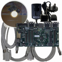
Board, Cables, CD, Power Supply
Processor To Be Evaluated
AT91SAM9G20
Data Bus Width
32 bit
Interface Type
RS-232, Ethernet, USB
Core
RISC
Silicon Manufacturer
Atmel
Core Architecture
ARM
Core Sub-architecture
ARM926EJ-S
Silicon Core Number
AT91SAM9G20
Silicon Family Name
ARM
Kit Contents
Board CD Docs
Rohs Compliant
Yes
For Use With/related Products
AT91SAM9G20
Lead Free Status / RoHS Status
Lead free / RoHS Compliant
Available stocks
Company
Part Number
Manufacturer
Quantity
Price
Company:

Part Number:
AT91SAM9G20-EK
Manufacturer:
Atmel
Quantity:
135


6.1
6.2
6.3
AT91SAM9G20-EK Evaluation Board User Guide
Wrong Silkscreen of BB and 1.0V on the Board
Choice of an Oscillator Capacitance
SD Card Slots and Booting Capability
There is a silkscreen reversion on the board, for the selection of the VDDBU source:
This erratum is not applicable for AT91SAM9G20-EK Rev. C and later versions.
For many reasons at the manufacturing level, Atmel does not specify any crystal references at the board
design stage.
Because of that, the user can find an inconsistency in the value of the used capacitance of the
18.432 MHz crystal on each pin (C23, C24), and the nominal load capacitance of the crystal.
As a reminder, here is the way to select these values.The electrical parameter allows you to fit the right
values provided by the crystal manufacturer - and not by Atmel. They are called "Load Capacitance" of
the crystal. You have to take stray capacitances (package, socket, trace) into account in order to be
close enough to the equivalent nominal Load Capacitance.
With the on-board HCM49-18.432MABJT crystal reference, 10 pF capacitances have been fitted on the
18.432 MHz crystal for a nominal 27 pF load capacitance.
On the board, Slot J13 is incorrectly marked with a “bootable” mention (solder side). This should be
applied to J35 instead. However, the schematic entitled ” Memory” attached to this User Guide, in
tion 5.1 ”Schematics”
On J10 position 1-2, the marking should be ‘BB’ for Battery Backup instead of ‘1.0V’
On J10 position 2-3, the marking should be ‘1.0V’ instead of ‘BB’.
does represent the correct location and marking.
6413C–ATARM–18-Feb-09
Section 6
Errata
Sec-
6-1
Related parts for AT91SAM9G20-EK
Image
Part Number
Description
Manufacturer
Datasheet
Request
R

Part Number:
Description:
MCU, MPU & DSP Development Tools KICKSTART KIT FOR AT91SAM9 PLUS
Manufacturer:
IAR Systems

Part Number:
Description:
DEV KIT FOR AVR/AVR32
Manufacturer:
Atmel
Datasheet:

Part Number:
Description:
INTERVAL AND WIPE/WASH WIPER CONTROL IC WITH DELAY
Manufacturer:
ATMEL Corporation
Datasheet:
Part Number:
Description:
Low-Voltage Voice-Switched IC for Hands-Free Operation
Manufacturer:
ATMEL Corporation
Datasheet:
Part Number:
Description:
MONOLITHIC INTEGRATED FEATUREPHONE CIRCUIT
Manufacturer:
ATMEL Corporation
Datasheet:
Part Number:
Description:
AM-FM Receiver IC U4255BM-M
Manufacturer:
ATMEL Corporation
Datasheet:
Part Number:
Description:
Monolithic Integrated Feature Phone Circuit
Manufacturer:
ATMEL Corporation
Datasheet:
Part Number:
Description:
Multistandard Video-IF and Quasi Parallel Sound Processing
Manufacturer:
ATMEL Corporation
Datasheet:
Part Number:
Description:
High-performance EE PLD
Manufacturer:
ATMEL Corporation
Datasheet:
Part Number:
Description:
8-bit Flash Microcontroller
Manufacturer:
ATMEL Corporation
Datasheet:
Part Number:
Description:
2-Wire Serial EEPROM
Manufacturer:
ATMEL Corporation
Datasheet: