DM300018 Microchip Technology, DM300018 Datasheet - Page 95
DM300018
Manufacturer Part Number
DM300018
Description
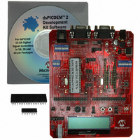
BOARD DEMO DSPICDEM 2
Manufacturer
Microchip Technology
Type
MCUr
Specifications of DM300018
Contents
*
Processor To Be Evaluated
dsPIC30F
Interface Type
RS-232
Silicon Manufacturer
Microchip
Core Architecture
DsPIC
Core Sub-architecture
DsPIC30
Silicon Core Number
DsPIC30F
Silicon Family Name
DsPIC30F2xxx, DsPIC30F3xxx
Lead Free Status / RoHS Status
Not applicable / RoHS Compliant
For Use With/related Products
dsPIC30F
Lead Free Status / Rohs Status
Lead free / RoHS Compliant
Other names
Q2448034
Available stocks
Company
Part Number
Manufacturer
Quantity
Price
Company:

Part Number:
DM300018
Manufacturer:
MICROCHIP
Quantity:
12 000


© 2005 Microchip Technology Inc.
14.1.2
The left side of the dsPICDEM 2 Development Board includes sockets (U2B1 and
U2A1) for 28 and 40-pin devices, respectively, in the Motor Control family. The right
side of the board includes sockets (U1C1, U1B1 and U1A1) for 18, 28 and 40-pin
devices, respectively, in the dsPIC30F General Purpose and Sensor family of devices.
These sockets are concentrically arranged headers that allow supported devices in DIP
packages to be plugged directly into the development board.
Table 14-2 lists the devices accommodated by each socket.
TABLE 14-2:
The schematic for the general purpose and sensor device sockets is shown in Figure
A-2: “dsPICDEM™ 2 Development Board Schematic (Sheet 1 of 7)”. The
schematic for the motor control device socket is shown in Figure A-3: “dsPICDEM™
2 Development Board Schematic (Sheet 2 of 7)”.
14.1.3
Device clocking is provided by on-board crystal oscillators. A 7.3728 MHz crystal
oscillator(Y2) provides a system clock for the Motor Control family of devices. Another
7.3728 MHz crystal oscillator (Y5) provides a system clock for the General Purpose and
Sensor family of devices.
Through-holes and pads are provided for a user-furnished watch-type crystal and two
capacitors (Y3 and Y6) connected across pins SOSC1 and SOSC2 on the dsPIC30F
device. Such crystals may be used for real-time clock operation.
External clock connections are available for motor control devices at Y1 and general
purpose and sensor devices at Y4.
The schematics showing resistor and capacitor values for all oscillator options are
provided in Figure A-6: “dsPICDEM™ 2 Development Board Schematic (Sheet 5
of 7)”
14.1.4
An RJ11 header has been provided on the dsPICDEM 2 Development Board in
order to interface with device programmers and debuggers like MPLAB ICD 2
and PRO MATE™ 3. DIP switches in S2, S3 and S4 are provided to connect
the PRO MATE 3 or MPLAB ICD 2 In-Circuit Debugger to the programming and
debugging pins on the installed dsPIC30F device.
Switches within S2 should always be used to designate the device being programmed
by MPLAB ICD2. These switches connect the clock and data lines from ICD 2 to the
Programming and Default Debugging channels (PGC/EMUC and PGD/EMUD) on the
dsPIC30F device. In some instances, users may find that their application uses certain
peripherals multiplexed on either the PGC/EMUC or the PGD/EMUD pins. In such
cases, they may avail of alternate debugging channels, EMUC1 & EMUD1 or EMUC2
& EMUD2 or EMUC3 & EMUD3. The dsPICDEM 2 Development Board supports the
General Purpose and Sensor Family
U1A1
U1B1
U1C1
Motor Control Family
U2A1
U2B1
Header Label
dsPIC30F Device Sockets
Oscillators
Programming/Debugging
DEVICE/SOCKET LOCATIONS
dsPIC30F3014, 4013
dsPIC30F2012, 3013
dsPIC30F2011, 3012
dsPIC30F3011, 4011
dsPIC30F2010, 3010,4012
dsPIC30F Devices Accommodated
Hardware
DS51558A-page 89
Related parts for DM300018
Image
Part Number
Description
Manufacturer
Datasheet
Request
R

Part Number:
Description:
Manufacturer:
Microchip Technology Inc.
Datasheet:
Part Number:
Description:
Manufacturer:
Microchip Technology Inc.
Datasheet:
Part Number:
Description:
Manufacturer:
Microchip Technology Inc.
Datasheet:
Part Number:
Description:
Manufacturer:
Microchip Technology Inc.
Datasheet:
Part Number:
Description:
Manufacturer:
Microchip Technology Inc.
Datasheet:
Part Number:
Description:
Manufacturer:
Microchip Technology Inc.
Datasheet:
Part Number:
Description:
Manufacturer:
Microchip Technology Inc.
Datasheet:
Part Number:
Description:
Manufacturer:
Microchip Technology Inc.
Datasheet: