AD8224-EVALZ Analog Devices Inc, AD8224-EVALZ Datasheet - Page 24
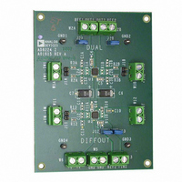
AD8224-EVALZ
Manufacturer Part Number
AD8224-EVALZ
Description
BOARD EVALUATION AD8224
Manufacturer
Analog Devices Inc
Specifications of AD8224-EVALZ
Channels Per Ic
2 - Dual
Amplifier Type
Instrumentation
Output Type
Single-Ended, Rail-to-Rail
Slew Rate
2 V/µs
-3db Bandwidth
1.5MHz
Current - Output / Channel
15mA
Operating Temperature
-40°C ~ 85°C
Current - Supply (main Ic)
750µA
Voltage - Supply, Single/dual (±)
4.5 V ~ 36 V, ±2.25 V ~ 18 V
Board Type
Fully Populated
Utilized Ic / Part
AD8224
Silicon Manufacturer
Analog Devices
Application Sub Type
JFET Input Instrumentation Amplifier
Kit Application Type
Amplifier
Silicon Core Number
AD8224
Kit Contents
Board
Lead Free Status / RoHS Status
Lead free / RoHS Compliant
Available stocks
Company
Part Number
Manufacturer
Quantity
Price
Company:

Part Number:
AD8224-EVALZ
Manufacturer:
Analog Devices Inc
Quantity:
135


AD8224
APPLICATIONS INFORMATION
DRIVING AN ADC
An instrumentation amplifier is often used in front of an ADC
to provide CMRR and additional conditioning such as a voltage
level shift and gain (see Figure 62). In this example, a 2.7 nF
capacitor and a 500 Ω resistor create an antialiasing filter for the
AD7685. The 2.7 nF capacitor also serves to store and deliver
the necessary charge to the switched capacitor input
of the ADC. The 500 Ω series resistor reduces the burden
of the 2.7 nF load from the amplifier. However, large source
impedance in front of the ADC can degrade the total harmonic
distortion (THD).
For applications where THD performance is critical, the series
resistor needs to be small. At worst, a small series resistor can
load the AD8224, potentially causing the output to overshoot
or ring. In such cases, a buffer amplifier, such as the
should be used after the AD8224 to drive the ADC.
±50mV
DIFFERENTIAL OUTPUT
The differential configuration of the AD8224 has the same
excellent dc precision specifications as the single-ended output
configuration and is recommended for applications in the
frequency range of dc to 1 MHz.
The circuit configuration, outlined in Table 4 and Table 7, refers
to the configuration shown in Figure 63 only. The circuit includes
an RC filter that maintains the stability of the loop.
The transfer function for the differential output is
where:
V
G
10µF
DIFF_OUT
=
Figure 62. Driving an ADC in a Low Frequency Application
1 +
1.07kΩ
+
49.4
0.1µF
= V
+IN
–IN
R
G
+OUT
kΩ
AD8224
+5V
− V
−OUT
REF
+2.5V
= ( V
500Ω
2.7nF
+IN
− V
−IN
) × G
AD7685
ADR435
AD8615
+5V
4.7µF
Rev. B | Page 24 of 28
Setting the Common-Mode Voltage
The output common-mode voltage is set by the average of +IN2
and REF2. The transfer function is
+IN2 and REF2 have different properties that allow the
reference voltage to be easily set for a wide variety of applications.
+IN2 has high impedance but cannot swing to the positive
supply rail. REF2 must be driven with a low impedance but
can go 300 mV beyond the supply rails.
A common application sets the common-mode output voltage
to the midscale of a differential ADC. In this case, the ADC
reference voltage is sent to the +IN2 terminal, and ground is
connected to the REF2 terminal. This produces a common-
mode output voltage of half the ADC reference voltage.
2-Channel Differential Output Using a Dual Op Amp
Another differential output topology is shown in Figure 64.
Instead of a second in-amp, ½ of a dual OP2177 op amp creates
the inverted output. Because the OP2177 comes in an MSOP,
this configuration allows the creation of a dual-channel,
precision differential output in-amp with little board area.
Errors from the op amp are common to both outputs and are,
thus, common mode. Errors from mismatched resistors also
create a common-mode dc offset. Because these errors are
common mode, they are likely to be rejected by the next
device in the signal chain.
V
CM_OUT
+IN
–IN
+IN
–IN
R
= ( V
G
Figure 64. Differential Output Using Op Amp
Figure 63. Differential Circuit Schematic
AD8224
+OUT
AD8224
+
–
REF
+ V
4.99kΩ
4.99kΩ
−OUT
AD8224
REF2
)/2 = ( V
–
+
–
OP2177
+IN2
20kΩ
+ V
33pF
V
REF
+
REF2
+OUT
+IN2
–OUT
+OUT
–OUT
)/2
Related parts for AD8224-EVALZ
Image
Part Number
Description
Manufacturer
Datasheet
Request
R

Part Number:
Description:
Single Supply, Rail to Rail Low Power FET-Input Op Amp
Manufacturer:
Analog Devices
Datasheet:

Part Number:
Description:
±1.7g Dual-Axis IMEMS Accelerometer Evaluation Board
Manufacturer:
Analog Devices Inc
Datasheet:

Part Number:
Description:
Inertial Sensor Evaluation System
Manufacturer:
Analog Devices Inc
Datasheet:
Part Number:
Description:
Manufacturer:
Analog Devices Inc
Datasheet:
Part Number:
Description:
Manufacturer:
Analog Devices Inc
Datasheet:
Part Number:
Description:
Manufacturer:
Analog Devices Inc
Datasheet:
Part Number:
Description:
Manufacturer:
Analog Devices Inc
Datasheet:
Part Number:
Description:
Manufacturer:
Analog Devices Inc
Datasheet:
Part Number:
Description:
Manufacturer:
Analog Devices Inc
Datasheet:
Part Number:
Description:
Manufacturer:
Analog Devices Inc
Datasheet:
Part Number:
Description:
Manufacturer:
Analog Devices Inc
Datasheet:
Part Number:
Description:
Manufacturer:
Analog Devices Inc
Datasheet:
Part Number:
Description:
Manufacturer:
Analog Devices Inc
Datasheet: