AD8224-EVALZ Analog Devices Inc, AD8224-EVALZ Datasheet
AD8224-EVALZ
Specifications of AD8224-EVALZ
Available stocks


Related parts for AD8224-EVALZ


AD8224-EVALZ Summary of contents
Page 1
... AD623 AD8222 1 Rail-to-rail output. to alleviate this problem, the AD8224 can operate on a ±18 V dual supply, as well single +5 V supply. The device’s rail- to-rail output stage maximizes dynamic range on the low voltage supplies common in portable applications. Its ability to run on a single 5 V supply eliminates the need for higher voltage, dual supplies. The AD8224 draws 750 μ ...
Page 2
... AD8224 TABLE OF CONTENTS Features .............................................................................................. 1 Applications ....................................................................................... 1 Functional Block Diagram .............................................................. 1 General Description ......................................................................... 1 Revision History ............................................................................... 2 Specifications ..................................................................................... 3 Absolute Maximum Ratings ............................................................ 9 Thermal Resistance ...................................................................... 9 ESD Caution .................................................................................. 9 Pin Configuration and Function Descriptions ........................... 10 Typical Performance Characteristics ........................................... 11 Theory of Operation ...................................................................... 20 Gain Selection ............................................................................. 20 Reference Terminal .................................................................... 21 REVISION HISTORY 5/10—Rev Rev. B Changes to Features Section............................................................ 1 Added Table 10 ...
Page 3
... OSI OSO T = −40°C to +85° −40°C to +85° ± ± −40°C to +85°C 300 T = −40°C to +85° − − ± 0.0001 Rev Page AD8224 Grade Max Min Typ Max 86 100 100 100 100 5 0.8 1 300 175 10 5 1200 ...
Page 4
... Differential and common-mode input impedance can be calculated from the pin impedance The AD8224 can operate diode drop below the negative supply; however, the bias current increases sharply. The input voltage range reflects the maximum allowable voltage where the input bias current is within the specification. ...
Page 5
... Table 4 displays the specifications for the Grade Conditions Min Typ 1500 800 120 14 ΔV = ±10 V step O 5 4.3 8.1 58 ΔV = ±10 V step O 6 4.6 9 Figure 63 . Rev Page AD8224 = ± Grade Max Min Typ Max 1500 800 120 14 5 4.3 8 4.6 9 ± Grade Max Min Typ ...
Page 6
... AD8224 − 2 25° REF A individual instrumentation amplifier configured for a single-ended output or dual instrumentation amplifiers configured for differential outputs as shown in Figure 63. Table 5. Individual Amplifier in Single-Ended Configuration or Dual Amplifiers in Differential Output Configuration Parameter COMMON-MODE REJECTION RATIO (CMRR) CMRR with 1 kΩ Source Imbalance ...
Page 7
... Differential and common-mode impedance can be calculated from the pin impedance The AD8224 can operate diode drop below the negative supply, but the bias current increases sharply. The input voltage range reflects the maximum allowable voltage where the input bias current is within the specification. ...
Page 8
... AD8224 − 2 25° REF A dynamic performance of each individual instrumentation amplifier. Table 6. Dynamic Performance of Each Individual Amplifier—Single-Ended Output Configuration, V Parameter DYNAMIC RESPONSE Small Signal Bandwidth − 100 G =1000 Settling Time 0.01 100 G =1000 Settling Time 0.001 100 G =1000 Slew Rate ...
Page 9
... Maximum Power Dissipation The maximum safe power dissipation for the AD8224 is limited by the associated rise in junction temperature (T approximately 130°C, which is the glass transition temperature, the plastic changes its properties. Even temporarily exceeding this temperature limit may change the stresses that the package exerts on the die, permanently shifting the parametric performance of the amplifiers. Exceeding a temperature of 130° ...
Page 10
... AD8224 PIN CONFIGURATION AND FUNCTION DESCRIPTIONS NOTES 1. THE AD8224 COMES IN TWO PACKAGE TYPES—EACH LEAD Table 11. Pin Function Descriptions Pin Number Mnemonic 1 −IN1 +IN1 REF1 7 REF2 8 − +IN2 −IN2 13 − OUT2 15 OUT1 –IN1 1 PIN 1 12 –IN2 INDICATOR AD8224 TOP VIEW +IN1 4 ...
Page 11
... GAIN = 100 BANDWIDTH ROLL-OFF 100 GAIN = 1 GAIN = 10 GAIN = 100/GAIN = 1000 10 GAIN = 1000 BANDWIDTH ROLL-OFF 100 1k FREQUENCY (Hz) Figure 7. Voltage Spectral Density vs. Frequency XX 5µV/DIV XX XX XXX (X) Figure 8. 0 RTI Voltage Noise ( 1µV/DIV XX XX XXX (X) Figure 9. 0 RTI Voltage Noise (G = 1000) AD8224 10k 100k 1s/DIV XX 1s/DIV XX ...
Page 12
... AD8224 4.5 4.0 3.5 3.0 2.5 2.0 1.5 1.0 0 TIME (s) Figure 10. Change in Input Offset Voltage vs. Warmup Time 150 GAIN = 1000 130 GAIN = 100 110 GAIN = 10 90 GAIN = 100 1k FREQUENCY (Hz) Figure 11. Positive PSRR vs. Frequency, RTI 150 130 110 90 GAIN = 1 70 ...
Page 13
... GAIN = 1 1k 10k 100k 1M FREQUENCY (Hz) Figure 19. Gain vs. Frequency R = 2kΩ LOAD R = 10kΩ LOAD V = ±15V S –8 –6 –4 – OUTPUT VOLTAGE (V) Figure 20. Gain Nonlinearity LOAD R = 10kΩ LOAD V = ±15V S –8 –6 –4 – OUTPUT VOLTAGE (V) Figure 21. Gain Nonlinearity AD8224 10M 2kΩ ...
Page 14
... AD8224 R = 10kΩ LOAD V = ±15V S –10 –8 –6 –4 –2 0 OUTPUT VOLTAGE (V) Figure 22. Gain Nonlinearity 100 R LOAD R = 10kΩ LOAD V = ±15V S –10 –8 –6 –4 –2 0 OUTPUT VOLTAGE (V) Figure 23. Gain Nonlinearity 1000 18 +13V 12 ±15V SUPPLIES 6 –14.8V, +5.5V +3V –4.8V, +0.6V 0 ±5V SUPPLIES – ...
Page 15
... –1 +125°C –40°C –2 +25°C +85°C NOTES 1. THE AD8224 CAN OPERATE THE NEGATIVE SUPPLY, BUT THE BIAS CURRENT WILL INCREASE SHARPLY. +1 –40°C +25°C +85°C +125°C V – S – SUPPLY VOLTAGE (V) Figure 28. Input Voltage Limit vs. Supply Voltage –1 –40°C +25° ...
Page 16
... AD8224 –1 +125°C – +125°C V – (mA) OUT Figure 34. Output Voltage Swing vs. Output Current 47pF NO LOAD 100pF 20mV/DIV 5µs/DIV XX XX XXX (X) Figure 35. Small Signal Pulse Response for Various Capacitive Loads ± REF XX 47pF 100pF NO LOAD 20mV/DIV 5µs/DIV XX XX XXX (X) Figure 36. Small Signal Pulse Response for Various Capacitive Loads, ...
Page 17
... Figure 43. Small Signal Pulse Response kΩ 100 pF ± LOAD LOAD S REF 20mV/DIV XXX Figure 44. Small Signal Pulse Response kΩ 100 pF ± LOAD LOAD S REF 20mV/DIV XXX Figure 45. Small Signal Pulse Response kΩ 100 pF ± LOAD LOAD S REF AD8224 4µs/DIV = 0 V 4µs/DIV = 0 V 40µs/DIV = 0 V ...
Page 18
... AD8224 20mV/DIV XXX Figure 46. Small Signal Pulse Response kΩ 100 pF, V LOAD LOAD 20mV/DIV XXX Figure 47. Small Signal Pulse Response 10 kΩ 100 pF, V LOAD LOAD 20mV/DIV XXX Figure 48. Small Signal Pulse Response 100 kΩ 100 pF, V LOAD LOAD 4µs/DIV = 2.5 V ...
Page 19
... Figure 53. Differential Output Configuration: Gain vs. Frequency 100 SOURCE V OUT SMALLER TO 90 AVOID SLEW RATE LIMIT 80 70 MEASUREMENT 100k 10M Rev Page DIFF_OUT CMR = 20 log OUT V CM_OUT LIMITED BY SYSTEM 10 100 1k 10k 100k FREQUENCY (Hz) Figure 54. Differential Output Configuration: Common-Mode Output (CMR ) vs. Frequency OUT AD8224 1M ...
Page 20
... AD8224 gain bandwidth product increases with gain, resulting in a system that does not experience as much bandwidth loss as voltage feedback architectures at higher gains. GAIN SELECTION Placing a resistor across the R AD8224. This is calculated by referring to Table using the following gain equation Rev Page 20kΩ NODE F ...
Page 21
... Package Considerations 50.40 The AD8224 is available in two version s of the 16-lead × 100 LFCSP package: with or without an exposed paddle. Blindly 199.4 copying the footprint from another 4 mm × LFCSP part 495.0 is not recommended because it may not have the same thermal 991 ...
Page 22
... A stable dc voltage should be used to power the instrumentation amplifier. Noise on the supply pins can adversely affect performance. The AD8224 has two positive supply pins (Pin 5 and Pin 16) and two negative supply pins (Pin 8 and Pin 13). While the part functions with only one pin from each supply pair connected, both pins should be connected for specified performance and optimum reliability ...
Page 23
... BIAS RF INTERFERENCE RF rectification is often a problem in applications where there are large RF signals. The problem appears as a small dc offset voltage. The AD8224 by its nature has gate capacitance (C inputs. Matched series resistors form a natural low-pass filter that reduces rectification at high frequency (see Figure 60). +15V 0.1µ ...
Page 24
... For applications where THD performance is critical, the series resistor needs to be small. At worst, a small series resistor can load the AD8224, potentially causing the output to overshoot or ring. In such cases, a buffer amplifier, such as the should be used after the AD8224 to drive the ADC. +5V + 10µF 0.1µ ...
Page 25
... All cables have a certain capacitance per unit length, which varies widely with cable type. The capacitive load from the cable may cause peaking in the AD8224 output response. To reduce peaking, use a resistor between the AD8224 and the cable. Because cable capacitance and desired output response vary widely, this resistor is best determined empirically. A good starting point is 50 Ω ...
Page 26
... AD8224 OUTLINE DIMENSIONS PIN 1 INDICATOR 12° MAX 1.00 0.85 0.80 SEATING PLANE PIN 1 INDICATOR 1.00 0.85 0.80 SEATING PLANE 4.00 0.60 MAX BSC 3.75 EXPOSED BSC SQ PAD 0. BSC TOP VIEW 1.95 BCS BOT TOM VIEW 0.80 MAX 0.65 TYP 0.05 MAX ...
Page 27
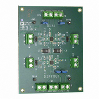
... AD8224HACPZ-WP −40°C to +85°C AD8224HBCPZ-R7 −40°C to +85°C AD8224HBCPZ-RL −40°C to +85°C AD8224HBCPZ-WP −40°C to +85°C AD8224-EVALZ RoHS Compliant Part. Product Description 16-Lead LFCSP_VQ 16-Lead LFCSP_VQ 16-Lead LFCSP_VQ 16-Lead LFCSP_VQ 16-Lead LFCSP_VQ 16-Lead LFCSP_VQ ...
Page 28
... AD8224 NOTES ©2007–2010 Analog Devices, Inc. All rights reserved. Trademarks and registered trademarks are the property of their respective owners. D06286-0-5/10(B) Rev Page ...